Make sure your enclosure has a proper seal or water, dust, and other debris may enter, causing reliability problems.
When it comes to PCBA manufacturing, take the time to consider all the challenges and risks you face. When you anticipate possible roadblocks ahead, you can establish milestones more efficiently and avoid backtracking with customers and stakeholders, an action that might harm your reputation.
As PCBA systems become more integrated with advances in technical standards, the design architecture naturally becomes more complex. Customers continue to demand advanced technical features for their solutions as functions get consolidated into smaller spaces.
There is, however, a way to control design complexity. A system’s manufacturability depends on design decisions made early in the project’s life cycle. Take a look at these top five PCBA design mistakes that can create unnecessary complexity in PCBAs, and how you can mitigate them.
Not Designing for Manufacture
In addition to all the functional and technical design requirements, a new design’s ability to go into production must be a final stakeholder requirement. Therefore, it is crucial to plan for manufacturing early in the process. Your contract manufacturing (CM) partner can assist you in completing an overall design for manufacturing (DFM) plan to ensure success.
The DFM will form the plan for all design aspects needed for production. All Bill of Materials (BoM), alternate components, prototype planning, and manufacturing technologies get outlined within the DFM. It will include specific processes for new vendor partners if they have unique requirements related to their technology. Complete this plan early in the project to avoid costly complexities later.
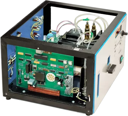
Product Enclosure Is Unmanufacturable
A product’s housing can be just as important to your project success as the PCBA located within it. Make sure your enclosure has a proper seal or water, dust, and other debris may enter, causing reliability problems.
A co-simulation of both the electrical and mechanical design structures should be completed in tandem. This integrated ECAD/MCAD simulation will ensure that connectors, harnesses, and other three-dimensional interfaces mate correctly without mechanical interference.
The complete design gets vetted during the first prototype build as proof that the co-simulation was successful. The DFM should consider any iterative changes and re-testing for final validation before moving forward.
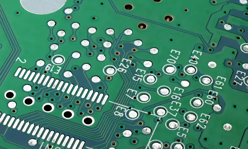
Incorrect PCB Landing Patterns
Incorrect landing patterns are common PCBA design mistakes
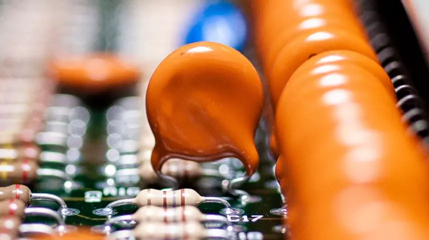
Every component has a manufacturer’s recommended and documented PCB solder pad pattern shape. Pin size, pin pitch, and whether underfill material will be used beneath the component for rigidity all contribute to pad structure. As smaller geometry components proliferate, some landing patterns can get swapped, but follow the details of each pad to prevent SMT issues.
If incorrect PCB landing patterns get used, the potential for the component to have open pins due to incomplete solder application increases. Cold solder joints or solder bridging between pads can also result. There is a potential for incorrect SMT issues to surface during prototyping unless the pads get checked against the manufacturer’s recommendations. DFM plans should include steps for checking for these issues prior to building.
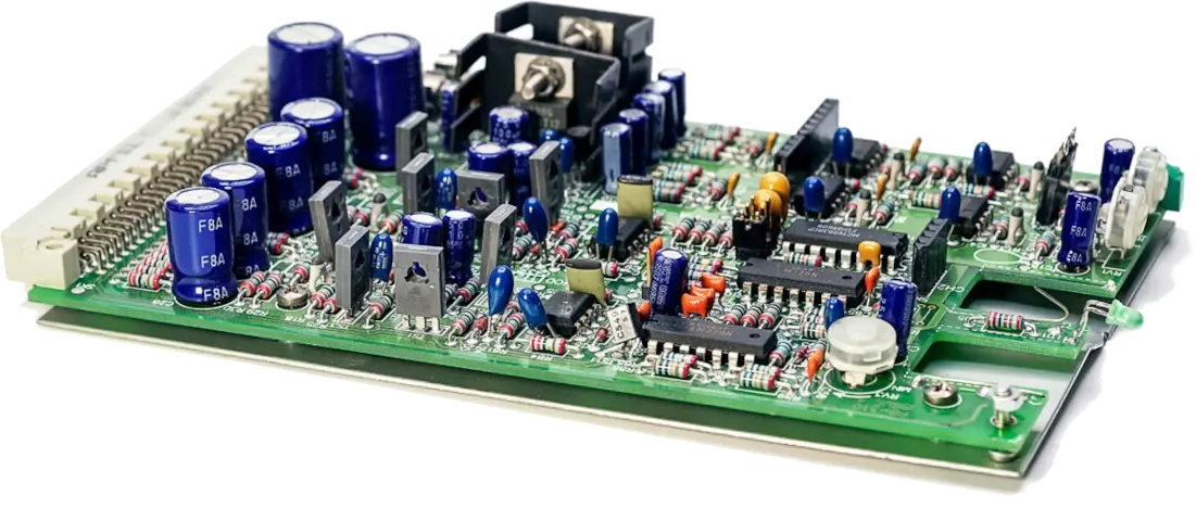
Decoupling Capacitors in Wrong Position
Decoupling capacitors primarily serve a few specific functions:
- AC couple a signal to remove the DC component using a series capacitor
- Removing AC noise from a power supply signal that needs to be electrically quiet
- Act as a low-pass or high-pass filter to a signal that could be wider in frequency than required
But a decoupling capacitor’s position relative to its companion component is crucial. Too far away, they have no effect. If they are too close, they may interfere with other components’ placement and mounting.

If their signal needs to reach a companion component, consider placing decoupling capacitors on the opposite side of the PCB, using a via. For accurate placement, their position should be checked and validated during the design phase. This may not be the most important step, but it must be verified prior to the final PCB tape-out for fabrication.
No Design Review
An inspection of the completed design against the original requirements and its manufacturing feasibility should get conducted at the end of every project. Without this formal step, good intentions get lost and informal understandings have the potential for error. The DFM will outline the design review items against manufacturability. Design reviews can be compared to court trials where evidence is presented to prove that the design itself is not in violation of manufacturing standards. Design teams often serve as ‘defense attorneys’ for their design when facing a review by other stakeholders who have an interest in its success.
Read about more common PCBA design errors and how to avoid them now.

Conclusion
Although new advancements can increase the technology used with designs, unbounded complexity should be tempered. Managing the complexity of your solution is possible. It is important to establish a clear DFM at an early stage with your CM partner’s involvement. Throughout the development stage, the design should be reviewed and tested against mechanical enclosures, PCB landing patterns, and passive component placements. It is possible for these items, as well as others, to cause unwanted problems in the future. Issues can be remedied in advance when intentionally incorporated into your DFM.
Improve Your Design Processes
Learn more about using integrated ECAD/MCAD