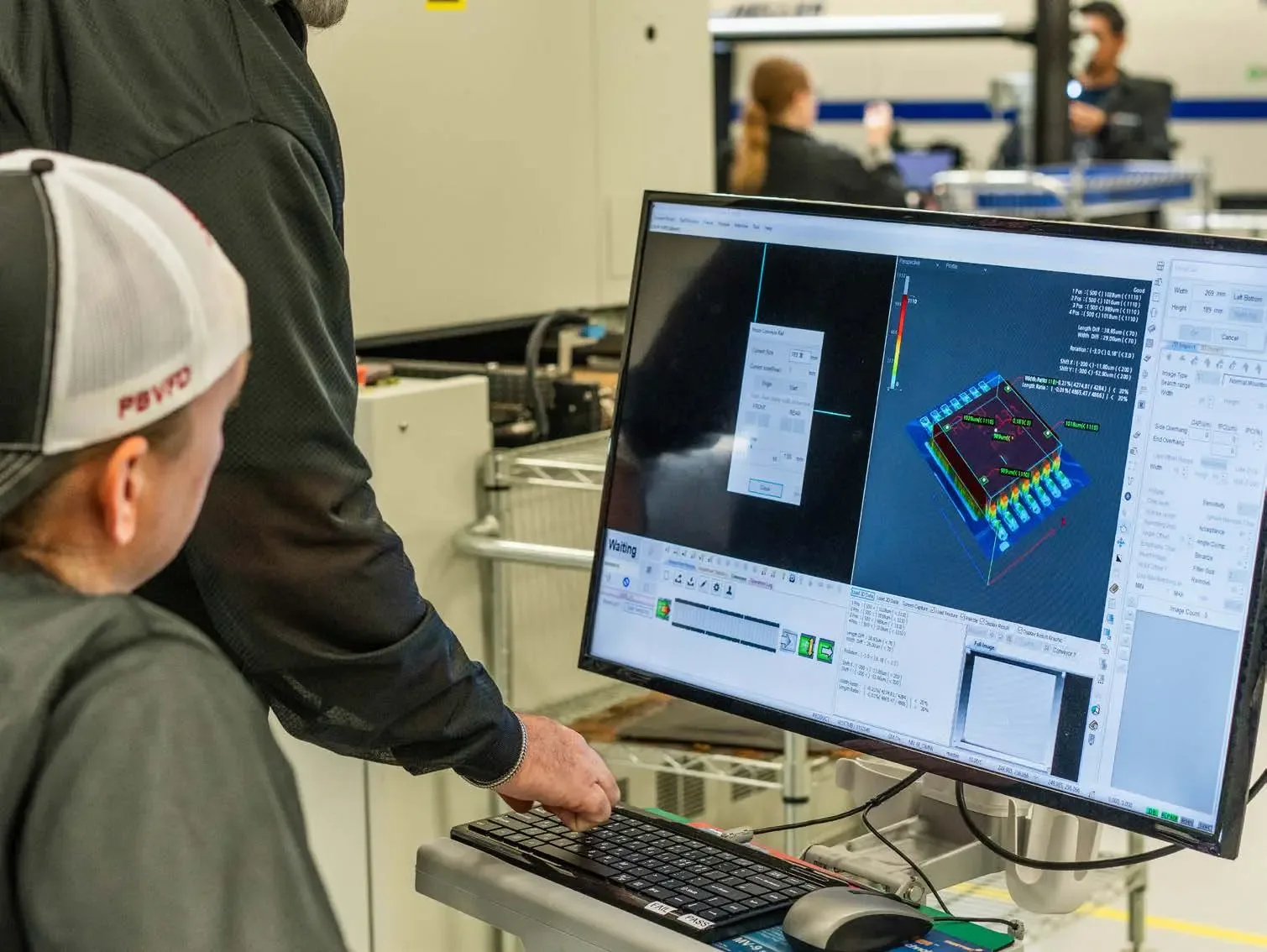
Fab Insights: Preventing High-Speed Routing Problems
In our previous installment, "Fab Insights: A Practical Guide to Impedance Control and High-Speed Routing,” we explored the fundamentals of impedance control and its critical role in ensuring signal integrity for high-speed circuits. This follow-up dives deeper, providing actionable tips and best practices to prevent common high-speed routing problems and achieve optimal board performance.
This article assumes you've grasped the core concepts from the first blog post. If you haven't yet, we highly recommend reviewing it for a strong foundation before proceeding.
Now, let's navigate the exciting yet intricate world of high-speed routing and ensure your designs operate flawlessly! You may be wondering if it is even possible to produce reliable high-speed circuits. I assure you that it is!
Achieving reliable signal integrity is a delicate process. Here, even minor details in the routing can have a significant impact on performance. Issues like crosstalk, reflections, and impedance mismatches have a detrimental effect on your carefully designed circuits.
Fortunately, by following a set of well-established best practices, we can mitigate these challenges. Let's explore some key techniques that will help you manage high-speed routing and guarantee your designs operate flawlessly.
- Use the three times trace width spacing rule to minimize coupling.
- The farther apart two traces are, the less likely there will be any leakage or signal coupling between them.
- If a trace is width X make sure other traces are at least 3X spaced apart.
Checkpoint
Achieving reliable signal integrity is a delicate process.
- Keep amplified signals away from their sources.
- Traces should maintain maximum space along their entire length.
- You may need to maintain distance among other components that those traces connect to.
- This will help prevent feedback loops from inadvertently forming due to coupling and cross-talk.
- Consider traces on different layers adjacent to one another through the board.
- If one trace carries a small signal make sure that no more powerful signals could couple or distort it.
- When routing signals on different layers be sure they are routed orthogonally to each other to reduce traces that are parallel and coupling.
- Think of all traces as series-connected inductors.
- The further apart the connections to a trace are, the more likely that inductive impedance will affect the voltage difference between the points.
- Reducing distances will improve performance and reduce problems.
- Keep traces on bypass capacitors as short as possible to minimize inductance.
- Provide efficient paths for return currents to ground.
- Signals will preferentially flow through the path with the least impedance.
- Avoid using 90 or acute-angle bends in traces.
- At high frequencies, these can lead to signal reflections.
- Signals that need to be synchronized should be length-matched.
- High-speed memory data busses, clock and data lines, and LVDS signaling should be matched.
Impedance Control Example
So, we know we need impedance control for high-speed signals and we know some best practices for routing the traces but we still need to calculate and match the impedance. Here is an example for routing the differential USB data signals for the RP2040 MCU. It is important to consider both the trace width and the spacing between the traces. The specified differential impedance for USB is 90 ohms which can be found on the hardware design document for the RP2040 on pages 10 and 11.
Steps to Calculate Trace Width and Spacing
Identify the Required Differential Impedance (Zdiff): The specified impedance, in this case, 90 ohms.
Determine Dielectric Constant (ϵrϵr): The relative permittivity of the dielectric material, for instance, FR4 (ϵrϵr around 4.5). The value depends on the specific material used.
Measure Trace Thickness (T): The thickness of the copper used in the PCB, often 0.035 mm for standard 1 oz copper.
Height of Dielectric (H): The height of the dielectric material between the trace and the ground plane, for example, 0.2 mm.
For differential pairs, the impedance is influenced by both the individual trace width (W) and the spacing (S) between the traces.
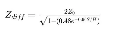
Differential Pair Impedance Calculation
The differential impedance (Zdifff) can be approximated using the following formula for a microstrip differential pair:

Where:
- Z0 is the characteristic impedance of a single-ended trace.
- S is the spacing between the two differential traces.
- H is the height of the dielectric material between the trace and the ground plane.
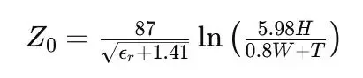
The characteristic impedance (Z0) for a single trace can be calculated using:

Example Calculation
Let's calculate the trace width (W) and spacing (S) for a differential pair with a 90-ohm differential impedance:
Given:
- Differential impedance (Zdif): 90 ohms
- Dielectric constant (ϵr): 4.5 (FR4 material)
- Trace thickness (T): 0.035 mm (1 oz copper)
- Height of dielectric (H): 0.2 mm
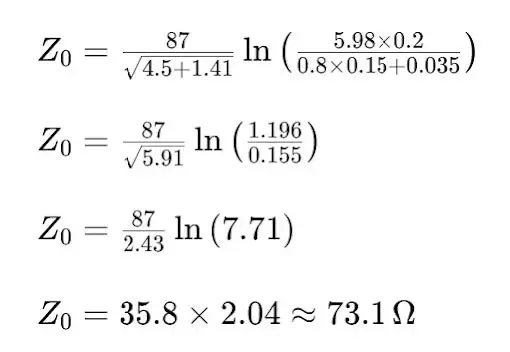
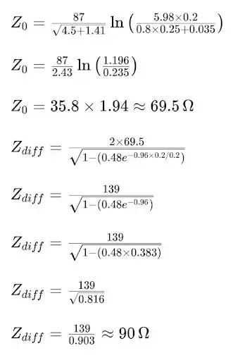
First, solve for the single-ended characteristic impedance (Z0):
Using an iterative approach, we start with an initial guess for W and S, then adjust until the desired Zdiff is achieved.
Initial Guess:
- Assume W=0.15 mm
- Assume S=0.15 mm
Calculate Z0 using the initial guess:
Calculate Differential Impedance
The initial guess results in a differential impedance higher than 90 ohms. We need to reduce Z0 by adjusting W and S.
Adjusting Parameters:
- Increase trace width (W) to reduce Z0.
- Increase spacing (S) to decrease Zdiff.
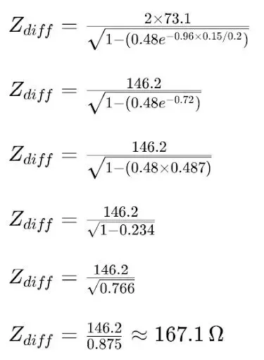
After several iterations of adjusting W and S and recalculating:
Final Parameters:
- Trace width (W): 0.25 mm
- Trace spacing (S): 0.2 mm
Final Calculation:
With these values, the differential impedance is approximately 90 ohms, meeting the USB specification for the RP2040 MCU.
Determining H in PCB Design
Standard Stack-Up Configurations: Many PCB manufacturers have standard stack-up configurations for different board thicknesses. These configurations specify the thickness of each dielectric layer and the copper layers. For example, a common configuration for a 4-layer PCB board might have a core and two prepreg layers with specific thicknesses.
Custom Stack-Up Requirements: For custom designs, you can specify the exact thickness of the dielectric layers to meet your impedance control requirements. This involves working closely with your PCB manufacturer to ensure the stack-up matches your design needs.
Consulting with Manufacturer: When in doubt, consult with your PCB manufacturer. They can provide detailed information about their standard stack-ups and the achievable tolerances for different materials. They can also help you determine the best stack-up to meet your impedance requirements.
Example Calculations Using a Common Stack-Up
Let’s consider an example where H is determined based on a typical four-layer PCB stack-up:
- Layer 1: Top signal layer
- Layer 2: Ground plane
- Layer 3: Power plane
- Layer 4: Bottom signal layer
Assume we have a standard four-layer stack-up with the following details:
- Prepreg Layer Thickness: 0.2 mm between the top signal layer and the ground plane
- Core Thickness: 1.2 mm between the ground plane and the power plane
- Prepreg Layer Thickness: 0.2 mm between the power plane and the bottom signal layer
For impedance calculations for traces on the top signal layer, H would be 0.2 mm, the thickness of the prepreg layer between the top signal layer and the ground plane.
Conclusion
High-speed routing is a major challenge for PCB designers. Even minor details can have devastating effects on your carefully crafted circuits. However, by following these best practices and collaborating with a knowledgeable PCB manufacturer like MacroFab, you can achieve flawless performance.
This post has equipped you with the knowledge to tackle high-speed routing challenges. Remember, meticulous planning and attention to detail are essential. Whether you're working with single-ended or differential signals, navigating dielectric materials, or conquering high-speed routing complexities, you now have the tools to ensure your designs function flawlessly at high speeds.
Related Topics
Fab Insights: A Practical Guide to Impedance Control & High-Speed Routing
A discussion on how understanding impedance control can result in successful prototyping and manufacturing when choosing to work with MacroFab.
Expert Tips for High-Speed Backplane PCB Design
Improve your high-speed backplane bus reliability with expert design tips.
High-Speed Routing Design: Tips for Engineers
Minimize undesirable parasitic effects occurring with high-speed signals. We cover stray inductors, dealing with crosstalk interference, and more.
Ready to start your next PCBA project?
Get an instant quote nowAbout MacroFab
MacroFab offers comprehensive manufacturing solutions, from your smallest prototyping orders to your largest production needs. Our factory network locations are strategically located across North America, ensuring that we have the flexibility to provide capacity when and where you need it most.
Experience the future of EMS manufacturing with our state-of-the-art technology platform and cutting-edge digital supply chain solutions. At MacroFab, we ensure that your electronics are produced faster, more efficiently, and with fewer logistic problems than ever before.
Take advantage of AI-enabled sourcing opportunities and employ expert teams who are connected through a user-friendly technology platform. Discover how streamlined electronics manufacturing can benefit your business by contacting us today.