MacroFab Blog
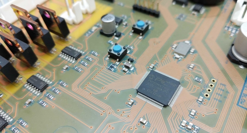
“High-speed routing” is an abbreviated description of routing copper traces on a printed circuit board in ways that minimize the undesirable parasitic effects that can occur with high-speed signals. A repeating signal could be considered High-Speed when the wavelength of signals frequency is equal to or less than four times the length of the trace that is carrying that signal.
For example, if you are routing a USB 3.0 SuperSpeed+ trace that can carry a 10 Gbit/s signal you will have to make sure your trace carrying the signal is under 7.5mm long. This would be tough to accomplish on most PCB designs thus your trace will need to be properly designed for High-Speed Routing to reduce problems.
Is This Only for RF Circuits?
The design of radio circuitry is complicated by the fact that all of the conductors in the circuit can act like transmitter antennas. These can radiate waves that can be “picked up” by other traces on the board and cause interference. Pairs of traces carrying a signal can also act like radio transmission lines, suffering from unwanted reflections and strange losses. Most of today’s electronic design revolves around microprocessors, embedded microcontrollers, FPGAs, digital circuits, digital audio processors, power amps, and motor controllers. This means we don’t need to worry about all of that RF “voodoo”, right?
Modern digital design
Well, let’s be careful here.
Do not make the mistake of thinking that digital systems are not affected by the problems that occur with RF circuits. The clock signal frequency in digital circuits and processors surpassed the RF range of frequencies years ago. However, the digital signals themselves are highly complex and involve very rapidly changing voltages which can trigger unwanted RF effects.
Read about the challenges of PCB RF Design now.
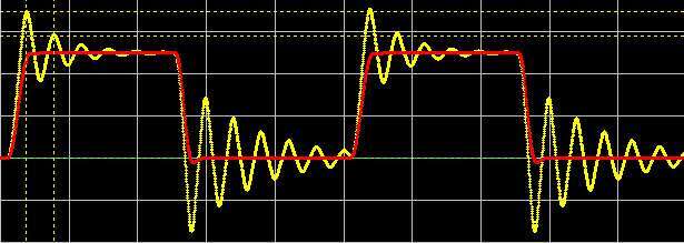
The majority of digital signals are square waves. From the Fourier Theory, we know that the sharp edges of square waves actually contain higher-order frequencies than the clock that drives the signal. A circuit board could suffer from significant problems from these higher frequencies and the digital signals can become distorted enough to cause a disruption of the operations of the circuit.
These higher frequencies can cause problems by distorting the leading and trailing edges of the signal, “blurring” the transitions from one digital state to the other. They can also cause false state transitions in the form of signal ringing.
What Kinds of Problems are Possible?
Before listing what problems are possible, let’s quickly review the concepts commonly used by RF engineers.
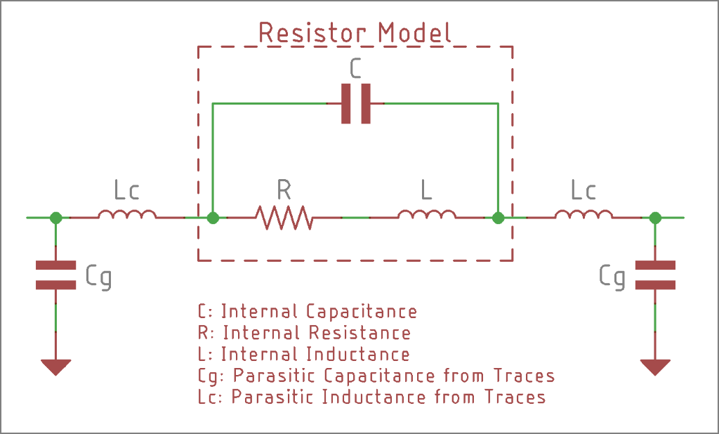
Impedance
Resistors are not the only electrical part that can create impedance. Capacitors and inductors create an impedance that depends on the geometric shape, the frequency of the signals passing through them, and part specifications. Copper traces also create small values of impedance.
Want to know more about impedance? Read How to Optimize PCBA Power Transfer with Parallel Impedance now.
Stray Capacitors
Capacitors can carry electrical current if it is continuously alternating. Capacitors can also conduct a variety of signal types as long as the voltage alternates. The capacitance value determines how much current can flow. This is the source of the impedance mentioned above for capacitors.
The geometry of the metal parts on a PCB will form unintended capacitors wherever two conductive surfaces face each other, with a non-conductive dielectric in between them (air, the PCB substrate, plastic, etc.,). The area of the two surfaces and the distance between them, and the non-conductive dielectric affect the capacitance that is formed.
Traces and signal paths on the PCB are susceptible to this parasitic capacitance effect. The PCB substrate plays the role of the capacitor’s non-conductive dielectric material in this case. PCB substrates are composed of fibrous materials woven into a sheet and then impregnated with a resin. The type of weave and resin employed can cause direction-dependent differences in the capacitance formed with the substrate in between.
Stray Inductors
Inductors are conductors wound into a coil. However, even straight copper traces will have some inductance. Bends and spiral shapes in trace pathways add to this inductance, and the presence of ferromagnetic material in components also increases the inductance.
Transmission Lines
A helpful way to model the parasitic effects of these capacitors, inductors, and resistances on traces is to treat the traces as a transmission line. Transmission line models are a standardized network of interconnected resistors, inductors, and capacitors with specific arrangements and values in accordance with the stray impedances that are typically formed as described above.
Current traveling down a transmission line is modeled as a wave of current, which is more accurate when we are in the high-speed or high-frequency range. Traveling wave phenomenon can occur in the transmission line which can create backward flowing reflections if an abrupt change in impedance is encountered by the signal as it travels along the transmission line. At higher frequencies, such reflections can completely eradicate the original signal or even damage the source driver.
Cross-talk interference
One of the most common issues that can occur in high-speed design is interference caused by a signal on one trace “leaking” onto another trace through an unintended parasitic capacitor that was formed between the traces. Sometimes cross-talk is caused by one trace acting as a transmitting antenna and the other trace acting as a receiving antenna. The space between the traces can be much larger in this case. Both situations create signals in places where they are not wanted, and such intruding signals are often tough to remove by secondary means such as filtering.
Unintended Attenuation of Signals
Stray inductors formed by the conductors can sometimes be large enough to produce a significant impedance to the flow of the signal through the conductors. This impedance will limit signal current just like an ordinary resistor. Frequency is very important here, and the magnitude of a trace’s impedance can be far greater at higher frequencies.
Reflections and Standing waves
As mentioned earlier, a signal encountering an abrupt change in impedance can experience a transmission line reflection phenomenon which can send a portion of the signal current backward, reducing the intensity of the forward wave. Depending upon the arrangement of the network, voltages or currents can build up to unexpectedly high values, potentially causing damage to components in the circuit.
Inconsistent Grounding
Traces that exhibit a high impedance can effectively defeat the purpose of the system ground by producing different ground potentials. Ground traces can become a chain of inductors connected in series, presenting a slightly different impedance to ground. The chain will cause each ground to be at a different voltage level than actual ground and different than any other “ground” connection. The differences produced depend on the total current flowing in the chain which can compound the problem. The circuit’s ground becomes unpredictable.
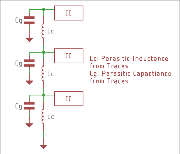
CHAIN GROUNDS 700x600
Most circuit designs assume that all connections to the ground are at the same voltage potential. Malfunctions and erratic behavior are almost guaranteed if ground connections are at different voltage levels like this. Circulating currents between grounding points at different voltage levels can also occur which creates ground loops. Inconsistent grounding can cause real havoc in circuit sections that have high gain by creating unwanted feedback paths which can stimulate unwanted oscillations.
Stephen and Parker talk to Jason Cerundolo about hardware layout tips for USB signals in this classic Circuit Break episode.
Propagation Time Delays
This effect becomes much more troublesome as the overall speed of the circuit increases to the point where the propagation time delays are comparable to the period of the clock signal. This makes it much more likely that individual bits will be lost due to synchronization issues.
How To Prevent High Speed Routing Problems
By now, you may be wondering if it is even possible to produce reliable high-speed circuits! I assure you that it is!
Careful consideration of this information during the development of the board design is the key. There are thousands of small decisions to make as a board design is developed and if the right choices are made in each of them, the resulting board design can be a solid performer in the high-speed domain.
Some general techniques for high-speed design are the following.
- Use the 3 times trace width spacing rule to minimize coupling.
- The farther apart two traces are, the less likely there will be any leakage or signal coupling of between them.
- If a trace is width X make sure other traces are at least 3X spaced apart.
- Keep amplified signals away from their sources.
- Maximum space should be maintained along the entire length of the traces.
- May need to be maintained distance among other components that those traces connect to.
- This will help prevent feedback loops from inadvertently forming due to coupling and cross-talk.
- Consider traces on different layers that are adjacent to one another through the board.
- If one trace carries a small signal make sure there are no more powerful signals that could couple or distort the signal.
- When routing signals on different layers be sure they are routed orthogonally to each other to reduce traces that are parallel and coupling.
- Think of all traces as series-connected inductors.
- The further apart the connections to a trace are, the more likely that inductive impedance will affect the voltage difference between the points.
- Reducing distances will improve performance and reduce problems.
- Keep traces on bypass capacitors as short as possible to minimize inductance.
- Provide efficient paths for return currents to ground.
- Signals are going to seek the path of the least impedance.
- Avoid using 90 or acute angle bends in traces.
- At high frequencies, these can lead to signal reflections.
- Signals that need to be synchronized should be length match.
- High-speed memory data busses, clock and data lines, and LVDS signaling should be matched.
Want more information? Read more practical PCBA design guidance on high-speed routing now.
Conclusion
There are many nuances to these techniques, and many volumes have been written on them. Most seem to condense down to the following:
Keep interference sources away from sensitive receivers, or put a shield between them. If there are signal receivers that assume that all signals propagate instantaneously, then make sure that they do, or redesign your receivers so that they can wait for out-of-sync data. If you have any questions or comments leave them below!
Related Topics
Fab Insights: Preventing High Speed Routing Problems
A continuation on the topic of impedance control and preventing high-speed routing problems. Diving deeper in achieving optimal board performance.
Ready to get started?
Sign Up TodayAbout MacroFab
MacroFab offers comprehensive manufacturing solutions, from your smallest prototyping orders to your largest production needs. Our factory network locations are strategically located across North America, ensuring that we have the flexibility to provide capacity when and where you need it most.
Experience the future of EMS manufacturing with our state-of-the-art technology platform and cutting-edge digital supply chain solutions. At MacroFab, we ensure that your electronics are produced faster, more efficiently, and with fewer logistic problems than ever before.
Take advantage of AI-enabled sourcing opportunities and employ expert teams who are connected through a user-friendly technology platform. Discover how streamlined electronics manufacturing can benefit your business by contacting us today.