Expert Tips for High-Speed Backplane PCB Design
Backplane PCBs are interconnect systems that integrate various electronic modules, creating a unified and scalable system. As IC bandwidths skyrocket, the need for high-speed backplane buses has grown significantly. Yet, they’re challenging to design.
These backplanes are crucial in sectors like defense, telecommunications, and data centers where high data transfer rates are essential. But herein lies the challenge: designers are met with intricate signal integrity concerns, including impedance control, lumped parasitics, and noise degradation.
Wondering how to enhance the reliability of your high-speed backplane bus? This article has the expert design tips you need. With a reliable system bus in place, you can focus on component functionality, assured that everything will sync seamlessly at the hardware level.
Design Considerations
A high-speed backplane is a sophisticated interconnection system, tailored to support data transmission at exceptionally high rates. But as data rates soar into the multi-gigabit range, signal integrity issues like crosstalk, impedance mismatches, and insertion losses become pronounced. This makes designing high-speed backplanes a tricky task.
Here’s a basic step-by-step for creating a high-speed backplane:
Step-by-Step Guide For Your High-speed Backplane PCBA Design

- High-Level Design with Functional Block Diagrams: At this phase, the objective is to capture the big picture of the system: how different components or circuit packs interconnect, the number of signals involved, power requirements, etc.
- Sketch a Preliminary Routing Outline: This involves a rough estimation of where tracks (connections) will go. It’s about understanding how tracks might be routed and identifying potential problems early on. Having a sense of the spatial layout can help in understanding the complexity of the design.
- Make a Pin-list Summary: Create a spreadsheet listing all the pins for every circuit module. This helps in estimating the number of layers required, organizing signals, selecting appropriate high- speed backplane connectors, and more.
- Select the Right Connectors: The connector is crucial. The choice can dictate design longevity and adaptability. Ensure it’s robust( since backplanes experience multiple insertions and removals), meets future high-speed requirements, and has the right pin configurations.
- Define the Geometry for Differential Pairs: Properly configure your differential pairs. Having consistent spacing and identical length traces within the pair reduces EMI and crosstalk and upholds characteristic impedance.
- Preliminary Stack-Up: This step involves deciding the arrangement of layers in a multi-stack high-speed backplane PCB.
- Make a Detailed Route Plan: Building on the preliminary routing plan, this phase involves a more detailed look at how the actual routes will run, ensuring that signals have clear paths and minimizing the potential for interference.
- Analyze Vertical Trace Space: Confirm there’s adequate room for traces to run vertically between connectors. This can influence your choice of connector or overall strategy.
- Conduct a Signal Clarity Check: Here, verify that your signals will travel cleanly without unwanted distortions. Utilize simulations and tools to ensure the integrity of your transmitted data.
Want more high-speed routing ideas? Read High-Speed Routing Design: Tips for Engineers now.
Challenges in High-Speed Backplane Design
As the signal travels from its source to its destination via a high-speed backplane, several factors can compromise its integrity. Here’s a breakdown of the core challenges faced:

- Conductor Skin Effects & Dielectric Losses: At high frequencies, signals prefer the outer “skin” of conductors rather than using its entire cross-section. This phenomenon is known as the “skin effect”. As the effective area of the conductor decreases, the resistance it offers to the signal increases, leading to signal loss. Also, the high-speed backplane PCB’s dielectrics are not perfect insulators and can absorb some of the signal’s energy.
- Return Loss & Impedance Discontinuities: The vias, connector pins, and differences in layer stacking on the backplane can introduce mismatches in impedance. When the signal hits these discontinuities, a part of it gets reflected back, diminishing the energy that reaches the endpoint.
- Signal Stubs: Stubs can cause parts of the signal to get trapped or delayed, leading to signal degradation and potential interference. Stubs are commonly caused by poorly designed vias, un-terminated branches in the trace routing, unused connector pins, elongated component leads, and mismatched layer transitions in the high-speed backplane PCB.
- Lumped Parasitics: Unintended resistances, capacitances, and inductances from components and board features can distort and degrade the signal.
- Noise Degradation On high-speed backplanes, daughterboards have multiple transceivers with differential pairs running parallel on the PCBA. When too close, they can cause crosstalk.
Tips for Better Signal Integrity in a High-Speed Backplane
To address the aforementioned signal integrity concerns, consider the following board design strategies:
- Choose the Right Equalizer: High-speed backplane links do not have a simple attenuation curve. They have multiple fluctuations due to reflections, crosstalk, and specific frequency resonances. Pick the right equalizer to compensate for these imperfections.
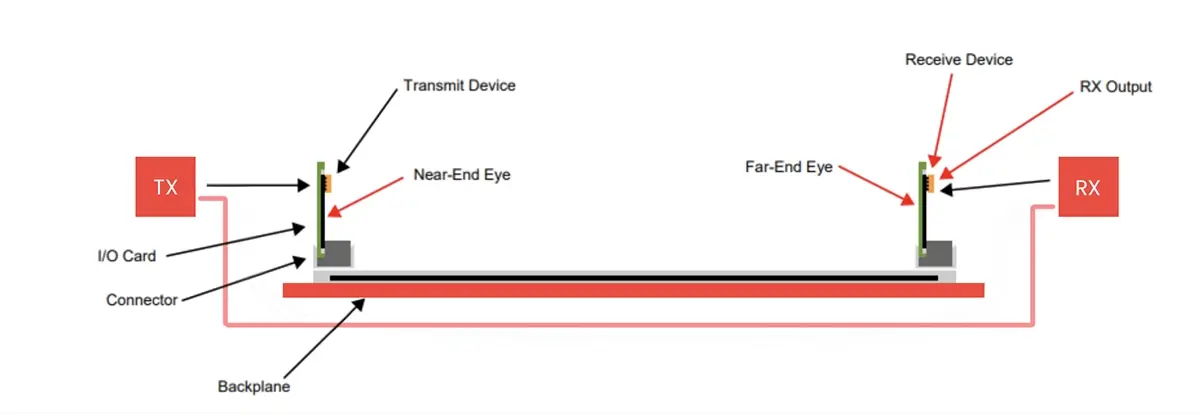
- Material and Component Evaluation: Pay attention to the choice of vias, stack-ups, and connector pins. These choices directly impact signal integrity. Always monitor the ‘eye-closure’ to gauge this effect.
- Prioritize High-Resolution Measurements: Always measure the high-speed backplane’s passive components as well as the near-end eye and far-end eye between daughter boards in both the frequency and time domains. A higher resolution in measurements means better pinpointing of potential issues like crosstalk or unexpected impedance changes.
- Use a Good Vector Network Analyzer (VNA): Ensure your VNA has an adequate frequency range, offers reliable time-domain performance, and provides a diverse set of de-embedding techniques.
- Manage the distributed capacitance on the Backplane: Capacitance on a backplane affects signal speed and quality. Over half of this capacitance originates from the transceiver’s input/ output pins. To improve signal integrity, select low-capacitance ICs for transceivers, increase trace impedance, and minimize stub lengths.
- Use a well-matched termination resistor: Place a termination resistor at the end of a signal trace to prevent reflections. Ensure its value matches the loaded impedance of the backplane trace for best signal integrity.
- Optimize for low-power consumption: For better power efficiency, reduce the backplane’s capacitance by using tighter slot spaces, shorter stubs, and low-capacitance components. This allows for higher termination resistor values, drawing less current.
- Incorporate Ground Pours for Enhanced Isolation: Use ground pours on your backplane PCB for better isolation and consistent impedance. This provides a stable ground reference, minimizing electromagnetic interference and ensuring strong signal integrity.
- Transform Unused Signal Layers into Plane Layers: Convert unused signal layers in multi- layered backplane PCBs to plane layers, either ground or power. This boosts electromagnetic interference shielding, aids heat dissipation, and can function as decoupling capacitors, reducing power noise and stabilizing impedance.
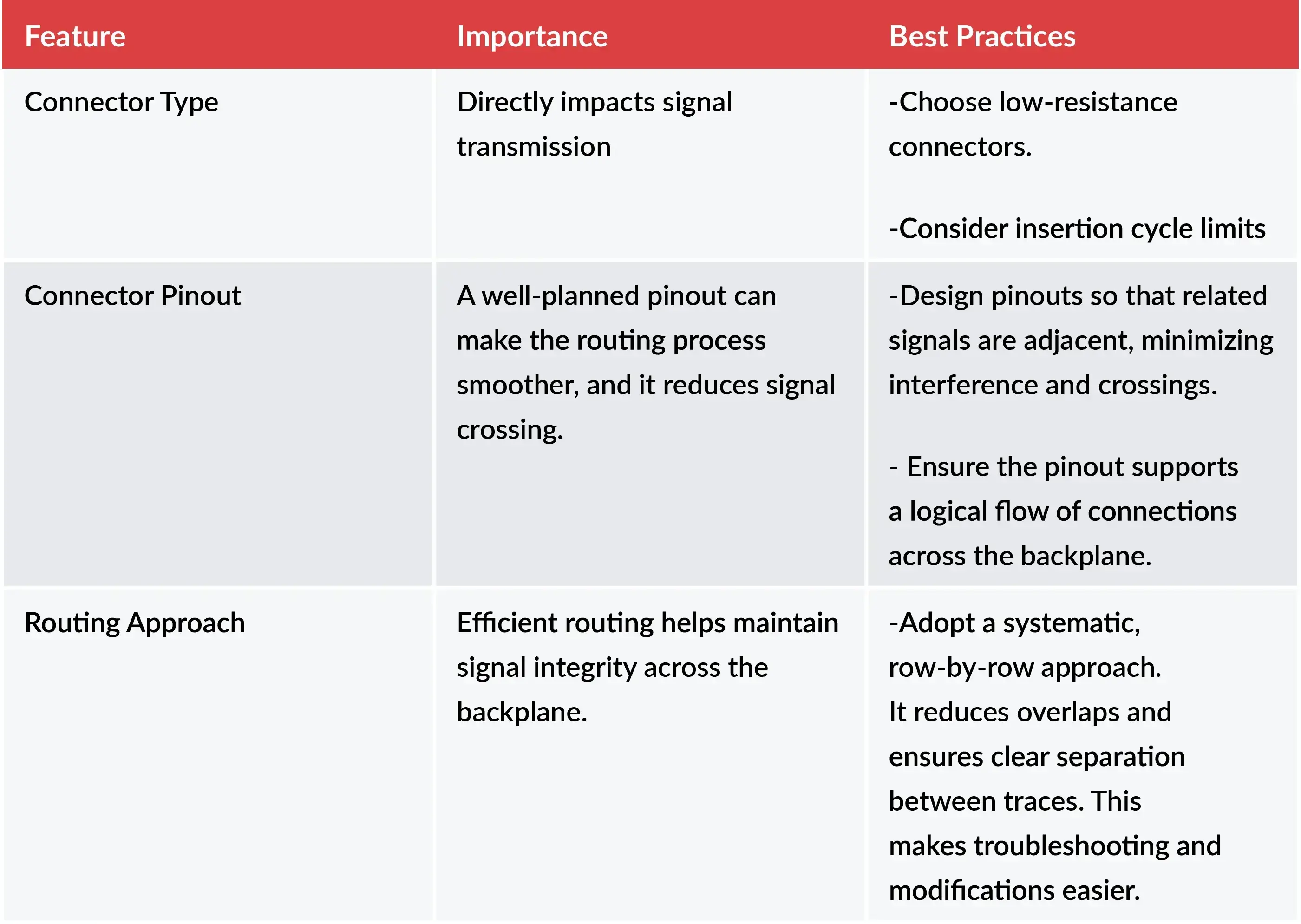
Connector, Pinout, and Routing Best Practices
A well-functioning high-speed backplane is heavily reliant on its connectors, pinouts, and routing techniques. Here are some best practices to consider:
Comparison Between Common Backplane Standards
Over the years, several standards have emerged, each tailored to specific application needs. Here’s a concise comparison of three prominent backplane standards: VME, CompactPCI, and VPX.
VME (VMEbus): The Versa Module Europa bus is an open-source backplane standard started in the 1980s. It was made so parts from different companies could work together in one system. While reliable, its parallel bus architecture makes it slower compared to newer technologies, especially for data-heavy tasks.
cPCI (CompactPCI): CompactPCI was introduced in the mid-1990s as an adaptation of the desktop PCI standard for industrial and embedded applications. It is particularly popular in telecom applications due to its high data rates and support for hot swapping.
VPX : VPX was developed in response to the growing demand for higher data transfer rates, particularly in the defense and aerospace sectors. Unlike older standards such as VME and CompactPCI, VPX adopts a switched fabric architecture, which directly addresses the limitations of traditional bus-based systems. This architecture not only facilitates multi-gigabit per second transfers but also enhances scalability and reduces contention.

Conclusion
High-speed backplanes are pivotal for designs that need fast data transfer. Different industries use specific backplane standards; for instance, the defense sector often opts for the Sensor Open Systems Architecture (SOSA).
However, crafting these backplanes is no easy task due to signal integrity challenges such as conductor skin effects, return loss, impedance discontinuities, signal stubs, and noise degradation. You need an expert design team and the right design tools in place, along with a reliable PCB manufacturer to get it right.
Related Topics
MacroFab vs. PCB Manufacturing Brokers: Why Direct Matters
This blog explores the key differences between MacroFab and manufacturing brokers, and why direct manufacturing is the optimal choice for PCBA needs.
Designing Rugged PCBAs for Smart City Applications
PCBA design in smart city applications have become a staple in making a change. From instances such as smart electric grids, crime detection, and waste.
Ultimate Guide To PCB Schematics: Concept to Prototype
A comprehensive guide for navigating early design phases and utilizing schematics alongside Gerber and drill files during the PCB creation process.
Having production challenges? Get help now.
Check out MacroFab's engineer-friendly featuresAbout MacroFab
MacroFab offers comprehensive manufacturing solutions, from your smallest prototyping orders to your largest production needs. Our factory network locations are strategically located across North America, ensuring that we have the flexibility to provide capacity when and where you need it most.
Experience the future of EMS manufacturing with our state-of-the-art technology platform and cutting-edge digital supply chain solutions. At MacroFab, we ensure that your electronics are produced faster, more efficiently, and with fewer logistic problems than ever before.
Take advantage of AI-enabled sourcing opportunities and employ expert teams who are connected through a user-friendly technology platform. Discover how streamlined electronics manufacturing can benefit your business by contacting us today.