Castellations: How to Use Them in PCBA Design
We will review what castellations are, why they get used, and several design considerations for castellated edges.
Checkpoint
With some foresight, most CAD design layout packages can accommodate castellated edge designs.
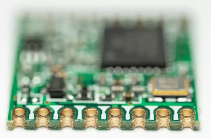
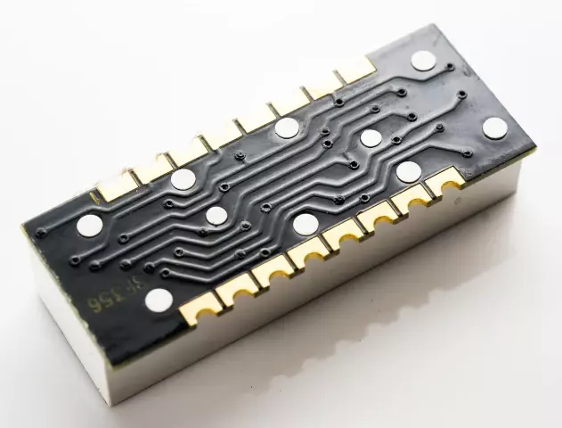
Many advanced system designs have criteria that require mounting an existing module onto a new PCBA. The best approach is to use a solder interface called castellations or a castellated edge. Semiplated copper indentations along the side of a PCBA provide both electrical and structural mounting support for a board-to-board interface.
There are several applications for this type of interface. We will review what castellations are, why they get used, and several design considerations for castellated edges.
What are Castellations?
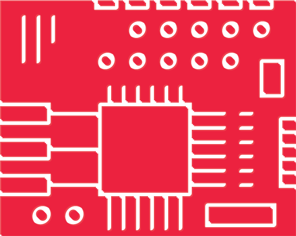
Connectors on rigid PCBAs do not use pins or solder balls. Instead, castellations bring the circuit nodes to the outside PCBA edges without any extra hardware.
Copper traces intended for connection to the outside follow the board’s edge. A hole gets drilled through the PCB within the copper trace. These holes are also known as annular rings or plated holes.
When the board gets separated from the array, the PCBA will get cut along its edge through these openings, forming a partial copper cavity–a castellation–which is electrically connected within the module circuit. Using these copper castellations as solder connections, the module can attach to a larger system board.
Why are Castellations Used
Castellations provide electrical connections from one PCBA to another. Smaller boards often serve as modules that provide a specific function to the system. For instances such as FCC-certified RF radio electromagnetic frequencies that get tested to specific standards, this can be especially useful. In this way, each module can get tested for known operation before the final system assembly.
Castellations also facilitate debugging during prototyping by bringing all module nodes into an accessible area and providing an easy SMT process for mounting modules.
Designing with Castellated Edges
PCBA design for castellations for SMT modules and system boards requires some minor planning. With some foresight, most CAD design layout packages can accommodate castellated edge designs.
A normal via process applies for developing the castellated holes on the PCBA edge. Holes get drilled through copper plating traces that extend beyond where the board edge will be eventually cut. Once the edge is cut to separate the PCBA from the rest of the array, these vias will resemble semicircle copper cylinders that span the thickness of the PCBA.
While castellated holes can be created in various ways with small cutouts and lead-in holes, the most popular method is to use the half-hole approach where a via within a copper trace is cut in half.
There are some design attributes for castellated holes to follow:
- Use appropriately sized vias that are larger than 0.5 mm, if possible.
- An ENIG surface finish is typically used for castellated vias to permit reduction of the diameters, but this design decision will depend upon the module’s application.
- To apply maximum solder paste to the top and bottom of the module, make sure you use the largest pad available.
- Allow for the proper spacing of the break tabs at the interface between the edge of the PCB and the rest of the array.
PCBAs on which modules will be mounted must have a footprint that is large enough to accommodate soldering castellated edges. The pads should be the largest dimensions allowed by the layout tool since their purpose is not only for electrical connection to the system but also for the structural mounting of the module. The area beneath the module must be kept free of components and other through-hole mountings since the module must sit flush with the PCB.
By using solder paste on the pads and solder masking where appropriate, the proper solder volume can be applied without the risk of cold or weak joints. Work with your CM partner during your project development to understand any other criteria needed for castellated mounting within your design for manufacturing (DFM) plan.
Conclusion
Integrated functional modules can be produced on a single assembled PCB using castellations that can be stacked on a larger board for a second assembly. The castellations provide both electrical and structural connections for the module as an SMT device. The SMT assembly process for a castellated module is like that of other surface mount devices.
Visual and electrical final test inspection can be accomplished on all castellated nodes after mounting, unlike other types of packaging with hidden pins.
During the design process, ensure that large annular rings are used both on the surface as well as the inner layers to strengthen the structure of the interface. Work with your CM partner to establish the use of the ENIG surface finish for the best results.
Finally, ensure that there is proper spacing for the break tabs that separate the PCBA from the array. This interface is critical to the success of the castellations
Related Topics
PCB Antenna Design: A Step-by-Step Guide
Step-by-step guide to the PCB antenna design process, providing practical tips to help you successfully integrate the antenna into your wireless product.
Top 10 Electronics Podcasts You Should Listen To
This curated list of top electronics podcasts is tailored for those trying to keep up with the rapidly evolving tech world.
MacroFab's Certifications Benefit PCBA Production
Your PCBA production must be secure and reliable for your products to compete in the market. We have listed our certifications and how they benefit you.
About MacroFab
MacroFab offers comprehensive manufacturing solutions, from your smallest prototyping orders to your largest production needs. Our factory network locations are strategically located across North America, ensuring that we have the flexibility to provide capacity when and where you need it most.
Experience the future of EMS manufacturing with our state-of-the-art technology platform and cutting-edge digital supply chain solutions. At MacroFab, we ensure that your electronics are produced faster, more efficiently, and with fewer logistic problems than ever before.
Take advantage of AI-enabled sourcing opportunities and employ expert teams who are connected through a user-friendly technology platform. Discover how streamlined electronics manufacturing can benefit your business by contacting us today.