FAB Insights: ENIG vs. ENEPIG
Let’s review ENIG vs. ENEPIG in a side-by-side comparison to identify the best option for your PCBA projects.
Checkpoint
Surface corrosion on “black pads” can lead to poor component solderability and a solder pad that loses connection to the component.
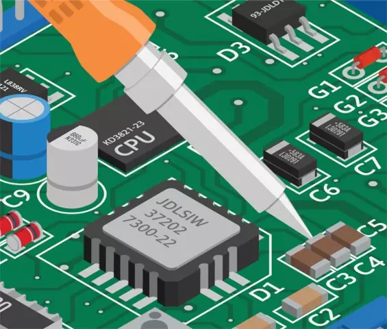
How to Choose PCBA Surface Finishes
Let’s review ENIG vs. ENEPIG in a side-by-side comparison to identify the best option for your PCBA projects. This blog will discuss the differences, advantages, and limitations of each.
ENIG (electroless nickel immersion gold) and ENEPIG (electroless nickel electroless palladium immersion gold) represent two of the main surface finish options to consider for your printed circuit board project. Surface finishes can stop the copper surface from oxidizing, maintaining excellent component solderability to guarantee the best electrical performance.
Working with a contract manufacturer (CM) such as MacroFab during your development process will help you identify the pros and cons of each method.
What is the ENIG PCB Finish?
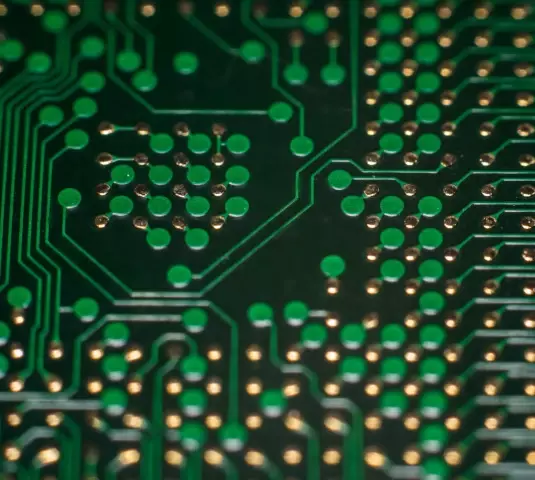
ENIG is MacroFab's default surface finish. ENIG has been a popular PCB surface finish for several decades due to its flat planar surface and reliability. This has been required for assembly due to the rise of tight-pitch BGA devices and other small surface-mount form factors. The process can also handle many solder reflow cycles with an extra benefit of a long shelf-life time.
However, historical PCB manufacturing challenges with some Electroless nickel immersion gold suppliers have caused nickel corrosion to form the “Black Pad” effect. This has been a leading weakness related to the ENIG surface finish, although a controllable one when proper measures are taken.
This “Black Pad” occurs when the nickel applied beneath the gold plating corrodes and resembles a black surface. This corrosion can lead to poor component solderability and a solder pad that loses connectivity to the component pad.
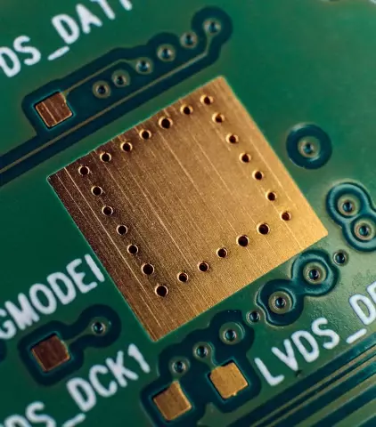
The ENIG surface finish can be challenging to produce for some PCBA manufacturers. When examining the final product, the gold application step can cover the final surface area which can obscure issues that cause “Black Pad”. The leading root cause analysis of this defect is that it is likely contamination of the Nickel which migrates into Gold and turns it a black color.
Your CM can rule out such issues through proper inspection; if no spikes or dark bands occur near nickel boundaries, a black pad is unlikely to occur. Additionally, a well-controlled nickel bath can minimize or eliminate the defect. Finally, working with a CM like MacroFab with a one-year workmanship guarantee provides extra peace of mind.
Advantages and Limitations of ENIG
An ENIG finish provides many advantages, including:
- A flat surface for fine-pitch BGA devices and other small form factor components.
- Excellent for in-circuit electrical test points and connectors with press-fit insertion posts.
- Support for wire bonding and edge card connections.
- Lower relative cost compared to ENEPIG finishes.
This finish also has limitations, including:
- Potential for “Black Pads” if the nickel and gold processing are not well controlled
- The PCB plating can be affected by the thickness of electroless nickel and gold
- A relatively low wet factor
What is ENEPIG Plating ?
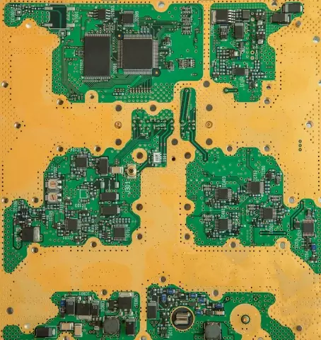
One simple solution to the black pad potential issue is to use an ENEPIG surface finish. ENEPIG stands for Electroless Nickel Electroless Palladium Immersion Gold. The ENEPIG finish solves this issue by depositing electroless palladium on top of the nickel layer. The palladium prevents any Nickel contamination from migrating to the gold.
ENEPIG deposits four individual layers of metal onto the printed circuit board. This process includes a copper layer that acts as a catalytic surface followed by an electroless nickel layer that provides a barrier layer. Then comes a layer of electroless palladium, which provides anti-oxidation and corrosion resistance properties and provides additional barrier protection. Finally, an immersion gold layer gets added to provide low contact resistance and to protect from friction and oxidation.
ENEPIG is suitable for PCBs using different packaging technologies soldered across the system board. ENEPIG can also satisfy a wide range of applications such as military, aerospace, and other high-performance devices within the medical industry that features high density and reliability.
While ENEPIG costs more than ENIG, it is still a cost-effective option that deposits thin layers of gold and palladium for additional durability and excellent solderability. Additionally, ENEPIG’s low contact resistance prevents energy losses, overheating, and poor grounding.
Advantages and Limitations of ENEPIG Plating
- Palladium mitigates the “Black Pad” quality issue seen with some CMs in the ENIG process
- Preferred for good solderability and many solder reflow cycles
- Highly reliable for wire bonding capability
- Satisfies the broad requirements of miniaturization, PCB thinness, and dense vias.
But Enepig also has its limitations. These include:
- Relatively higher cost than ENIG may not be economically suitable for all applications
- Reduced SMT Solder performance due to a thicker layer from palladium
- Longer duration to wet
Additional Surface Finishes and Their Characteristics
Other surface finishes to know about include:
- Lead-Free HASL(Hot Air Solder Leveling): This process involves coating the PCB with a tin/lead alloy, but in a lead-free version, tin is used with other metals like copper, nickel, or silver. It provides good solderability and is a cost-effective option for projects not requiring fine-pitch placement.
- Electrolytic Hard Gold (EHG): This surface finish involves the application of hard gold plating over a nickel layer. EHG is known for its exceptional durability and excellent conductivity, making it an ideal choice for high-wear areas such as edge connectors where frequent insertion and removal occur.
Learn more about surface finishes by listening to Grass Fed PCBs now.
Ready for more Fab Insights? Read Fab Insights: Preventing High-Speed Routing Problems now.
Conclusion
Both surface finishes offer excellent PCB planarity for systems that require tight-pitch components. While “Black Pad” issues may have plagued ENIG suppliers in the past, MacroFab has solved this quality challenge and can offer either finish without concern for quality. ENEPIG offers a more robust palladium application, it can also provide a higher reliability process for more demanding environmental applications.

When considering which surface finish to use, the following technical questions should be answered by working with MacroFab. These questions will have a role in influencing the selection of your optimal PCB surface finish for your project:
- Are lead-free solders, or the Reduction of Hazardous Substances (RoHS compliant), a requirement of your PCB design?
- What component form factor types and pin pitch will be used within the PCBA?
- Will the PCB have wire-bonded components or will they all be mounted using wave solder?
- To what environmental issues (temperature, humidity, and handling) will the final product be exposed?
While ENIG and ENEPIG are two of the more popular surface finish options, MacroFab also offers lead-free finishes like EHG and LF-HASL (lead-free Hot Air Solder Leveling) as PCB surface finish options. Lead-Free HASL may be an alternative for those systems that do not have fine-pitch device pins.
Related Topics
Fab Insights: HASL vs ENIG
Choosing the right surface finish for a PCBA can be tricky. HASL and ENIG differ in their methods of coating printed circuit boards.
Want More PCBA Design Tips?
Download “Design Faster, Improve Quality: Tips for PCBA Development."
About MacroFab
MacroFab offers comprehensive manufacturing solutions, from your smallest prototyping orders to your largest production needs. Our factory network locations are strategically located across North America, ensuring that we have the flexibility to provide capacity when and where you need it most.
Experience the future of EMS manufacturing with our state-of-the-art technology platform and cutting-edge digital supply chain solutions. At MacroFab, we ensure that your electronics are produced faster, more efficiently, and with fewer logistic problems than ever before.
Take advantage of AI-enabled sourcing opportunities and employ expert teams who are connected through a user-friendly technology platform. Discover how streamlined electronics manufacturing can benefit your business by contacting us today.