Top 10 Causes of Magic Smoke
The excitement of seeing your new circuit or PCB Assembly operating for the first time is deflated when one of the components releases your arch-nemesis – the magic smoke. While this can be frustrating, several areas for design review can mitigate this problem and should be part of your next design process to achieve functional success in the future. Let’s take a look at the top ten areas to prevent your boards from releasing magic smoke.
Make the Right Connections
Ahead of the system PCB fabrication tapeout, a detailed design overview for each component pin is needed. This includes not only power and ground pins but also all the digital I/O, control, analog, and do-not-connect (DNC) pins. The functional operation of each pin should be compared against the signal input device. The specified minimum and maximum voltage and current of each should be compared against the worst signal cases. DNC pins should be soldered to an open to maintain mechanical integrity.
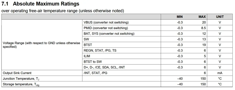
Datasheet excerpt from the Texas Instruments BQ25883 showing the voltage ranges for the components I/O.
EDA design software tools should do these comparisons (called ERC or Electronic Rule Checks) automatically, but the results will only be as good as the component library was built.
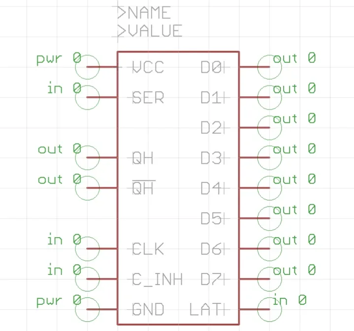
The Eagle EDA tool allows setting how certain pins should be used for ERC checks..
Taking the extra steps to set component pins aspects on the schematic symbol can save headaches down the road. A final pin review often identifies these subtle issues.
Take a Hard Look at the Mirroring
When designing component layouts, pay close attention to call outs on the mechanical drawings. The majority of components are drawn looking downwards at the component which is also the typical way EDA tools support drawing footprints. However, some components (electromechanical relays are one) are drawn from the bottom side. This has tripped up many design engineers.
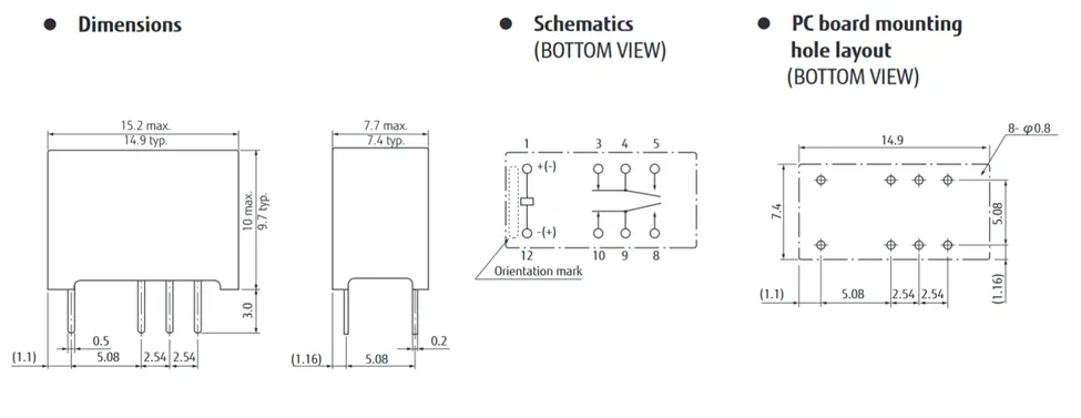
A relay layout denoting that the hole layout and schematics are from bottom view.
Doppelganger Components
All components, both active and passive, come in a variety of functional variants. Package form factor, tolerance, speed rating, pinouts, and power ratings are just some of the differences that can separate one similar component from another. Ensure that your BOM accurately describes the exact component variant that your design requires. Once your PCB Assembly is ordered, MacroFab will verify that the components' footprints match the PCB layout. Component variants look the same and will be hard for a contract manufacturer to catch as being a problem. Low dropout regulators frequently exhibit these variant pinout changes and traits.
Challenging Pitches
Narrow pitch Ball Grid Array (BGA) devices and Small Outline Transistor (SOT) components are efficient in minimizing system area. Resistors and capacitors smaller than 0201 dimensions are becoming more commonplace for new designs.
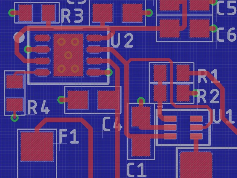
PCB layout showing solder pad openings with proper clearance.
Without proper solder pad openings and spacing on the layout, their small solder footprint can lead to bridging and cold solder joints. A review of the solder screenprint for the PCB Assembly should be completed against the assembly requirements to eliminate layout issues stemming from poor solder connections. Although layout tools should flag design rule violations (DRC) for spacing issues, specific assembly-challenged areas may need to be added to your ruleset. MacroFab reviews these potential problems with Design Rule Checks during our engineering review of your order and will notify you of issues.
(Don’t) Push it to the Limit
Active components may need a current limit on their respective pins to prevent excessive transient current events. Direct driving MOSFET gates with a microcontroller’s i/o is an example of this. It is also a good idea to calculate the current draw of your system and limit the current draw to this number on powering up the circuit for the first time to limit any potential damage.
Additional protection circuitry may be required to protect the system from surge current-type events that could damage the electronics. Whether the surge occurs at first power-up or is a discrete abnormal event, the intent is to protect the system from the offending signal. Often, this can be done with Zener diodes and other clamping or snubbing devices.
Poka-Yoke Protection
If the PCB Assembly is a sub-system within a larger, more complex system, the connectors and any cable interfaces should have a Poka-Yoke strategy to prevent mis-insertion. This approach creates a foolproof method to ensure that the system is properly connected. An everyday example of this is the three-prong electrical outlet plug in the USA that only affords one orientation for proper insertion
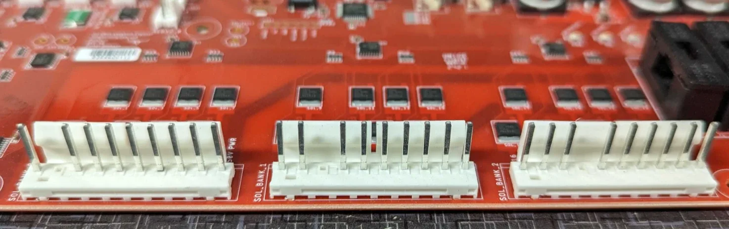
Connectors should be keyed and only allow one orientation and configuration to be plugged in.
Review Failure Modes and Address the Outside Concerns
A complex circuit may have many potential ways that it could fail, often including some that are not intuitive. Many organizations require a complete Design Failure Mode Effects Analysis (DFMEA) review to determine and review all these modes of operation that could fail. This is generally a good practice to identify weaknesses in the design and edge cases. After identification, each failure mode will be scored based on its severity, probability of occurrence, and method of detection. A risk priority number can be calculated to determine the most impactful failure types. The worst offenders should be addressed within the design or test methods to improve the system performance and reduce the opportunity for smoke.
An electrical system is not self-contained as it must accept interference from the external environment. A power surge, ground bounce, or EMF interference has the potential to damage the system. Large RF signals may damage radio receivers that are designed only to observe small signals without the proper filtering. Consider all of the worst-case signals during the system design – internal to the board, and external from the environment. Part of the system DFMEA review should ask the design team – “What outside electrical interference could cause this system to fail”?
Identify Initial Conditions
The initial start-up conditions for a system are often neglected. The steady-state operation is the most valuable and the mode that is given the most attention. This initial operation time may be the most severe, electrically, to the design. A proper design review should model all the transients and inrush current at turn-on. It is during this stage that capacitors first charge and transient spikes could be observed at the internal component pins. Microcontrollers enter a boot sequence where memory is read and initial activity takes place. The current consumption during this phase is higher and must be modeled during the design phase of the project. This unusual, but predictable, power activity could create scenarios where component maximum tolerances are exceeded.
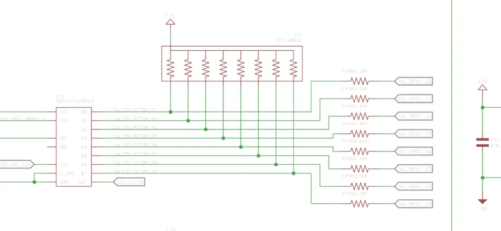
Outputs of a 74HC595 shift register pulled up to ensure power on signal state is deterministic.
While many digital I/O and control signals offer internal pull-up and pull-down resistors, some legacy components do not. Normally, a high or low signal will be driven with the proper termination on the other end of the transmission line. If neither a high nor low is driven, the pin has the potential to be left floating in a logical unknown or tri-state. This case can pull unwanted current and power from the supply when an entire digital bus is left in this state. An external resistor that is tied to GND or positive supply may be needed for those components that do not offer internal terminations or are driven by microcontrollers that take time to activate and drive signals. A supply line to an active component may also need a current limiter to prevent a runaway thermal situation where the component draws excessive current beyond its capability. Ensure your signals have determinate states on power on.
Inspect the Corners
While nominal conditions are the easiest to design for, the minimum and maximum scenarios cannot be ignored since they will be a required use case. The design must consider all of the corner cases of elevated supply, extreme temperatures, and environmental conditions such as humidity and EMC, maximum loading and computation.
Keep the Smoke Inside
The first verification step for a new circuit or PCB Assembly is to turn it on and check for unwanted smoke. Inadvertent errors can cause issues at this first step. Properly review the system requirements, layout, bill of materials, and corner cases to mitigate these issues. MacroFab can help you understand minimum pitch and assembly challenges in advance of fabrication. On your next design, make sure to keep the smoke inside the components and don’t let it out in the open.
Check out this episode of our podcast, Circuit Break, where we had industry leader, electrical engineer James Lewis on to discuss New Design Checklists and how to properly bring up new designs.
Related Topics
MacroFab vs. PCB Manufacturing Brokers: Why Direct Matters
This blog explores the key differences between MacroFab and manufacturing brokers, and why direct manufacturing is the optimal choice for PCBA needs.
Ultimate Guide To PCB Schematics: Concept to Prototype
A comprehensive guide for navigating early design phases and utilizing schematics alongside Gerber and drill files during the PCB creation process.
How MacroFab Uses Clear Communication to Improve Your PCB Production Experience
This blog will discuss how MacroFab can help customers in their PCB production experience through clear communication in a high-octane environment.
Ready to Build Something Great?
Get an Instant Quote TodayAbout MacroFab
MacroFab offers comprehensive manufacturing solutions, from your smallest prototyping orders to your largest production needs. Our factory network locations are strategically located across North America, ensuring that we have the flexibility to provide capacity when and where you need it most.
Experience the future of EMS manufacturing with our state-of-the-art technology platform and cutting-edge digital supply chain solutions. At MacroFab, we ensure that your electronics are produced faster, more efficiently, and with fewer logistic problems than ever before.
Take advantage of AI-enabled sourcing opportunities and employ expert teams who are connected through a user-friendly technology platform. Discover how streamlined electronics manufacturing can benefit your business by contacting us today.