How Poka Yoke Can Improve Your PCBA Design Process
Checkpoint
Quality is everyone's responsibility.

W. Edwards Deming, a renowned engineer, once emphasized, “Quality is everyone’s responsibility.” In electronics, this is especially true.
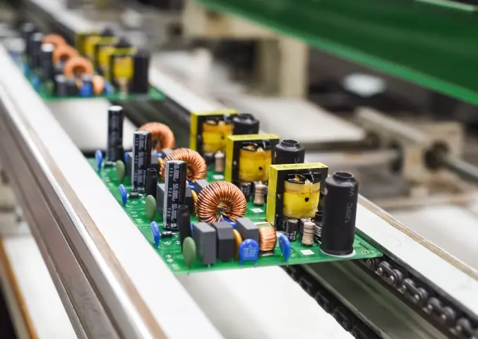
As someone involved in printed circuit board assembly (PCBA) design, you know just how vital quality is for creating reliable and efficient products. Even a small design flaw found after production can result in costly delays, rework, and negative customer feedback, damaging your reputation.
In this blog post, we will delve into essential aspects of incorporating Poka Yoke principles into PCBA design including Design for Manufacturability (DFM), and Clear Labeling and Documentation. Using these methods, you can significantly reduce errors and flaws in your products, ensuring they meet the high standards of quality, dependability, and performance that users expect.
To understand Poka Yoke’s core concepts, it’s essential to first distinguish between mistakes and defects.
Clarifying the Concepts: Mistakes vs. Defects
Although the terms ‘mistakes’ and ‘defects’ might initially appear synonymous, they embody separate nuances in meaning. A mistake denotes an error that occurs during a task’s execution, whereas a defect is the flawed output or product derived from such a mistake. In effect, a defect represents a mistake that has made its way to the customer.
Suppose you are designing a PCB layout and accidentally place a component too close to another, violating the minimum clearance requirements. This misplacement is a mistake.
Should the PCBA be produced without rectifying this error, potential defects could arise, such as electrical shorts, overheating, or even a diminished product lifespan. Therefore, by reducing errors during the design process, you simultaneously decrease the probability of defective PCBAs.
Poka-Yoke’s primary objective is to establish processes that either avert mistakes completely or rapidly detect and correct them. This is why it’s often referred to as “mistake-proofing.”
A Glimpse into Poka-Yoke’s Origins

Shigeo Shingo, a Japanese industrial engineer at Toyota, introduced Poka-Yoke in the 1960s. Back then, the manufacturing industry extensively used statistical process control (SPC) to oversee product quality, analyzing data to identify and adjust for variations. However, Shingo was discontented, realizing that SPC couldn’t fully eliminate defects. He sought a proactive approach to prevent errors at the outset.
During a 1961 visit to the Yamada electric plant, Shingo noticed assembly workers occasionally forgot a crucial spring in switches, resulting in defects. These errors weren’t always caught, leading to customer dissatisfaction and reputational harm.
Shingo recognized that solely depending on workers’ attentiveness was inadequate for error prevention. He advocated for a more robust process that, should a worker make an error, could be prevented or corrected before the product left the factory.
Inspired by these experiences, Shingo developed Poka-Yoke, reshaping the assembly process to lessen reliance on worker memory or skill for error prevention.
Prevention and Detection Poka Yoke Techniques

Poka-Yoke techniques can be classified into two main categories: prevention and detection.
Prevention techniques are designed to prevent errors from occurring in the first place. Detection techniques are designed to detect errors after they occur, so they can be corrected before they cause a problem.
Prevention techniques include designing parts so they can only be assembled correctly through keying or asymmetrical design, using sensors to detect when parts are in the wrong position, and using color coding or labeling to ensure that the right parts are used in the right place. PCBA designers commonly use asymmetrical or keyed connectors or software that detects clearance violations during layout to prevent incorrect connections.
Detection techniques include using warning lights or alarms to alert operators when a problem occurs, using automated inspection systems to detect defects, and using statistical process control to monitor the quality of the process.
By incorporating both types of Poka-Yoke techniques into your PCBA design process, you can significantly reduce defects and enhance the overall quality of your products.
Read about the five biggest PCBA design mistakes now, so you can avoid them later.
Poka Yoke Strategies for Mistake-Proofing
Poka Yoke techniques can significantly improve PCBA product quality, reduce rework costs, and enhance overall operational efficiency. Here are four ways you can utilize Poka Yoke principles to optimize your PCBA designs:
- Identify Potential Failure Points in Product Assembly: One of the core tenets of Poka Yoke is to scrutinize the assembly process, identifying areas where a product could fail if parts are not assembled correctly. In the context of PCBA, this involves conducting thorough risk analyses for each component and its position on the board. Should a resistor or capacitor be placed wrongly, for instance, the resulting malfunction could lead to significant downtime and financial loss. Utilize tools like Failure Mode and Effects Analysis (FMEA) to systematically detect potential points of failure and address them proactively, or work with your CM to take these steps.

- Prioritize Critical Features for Proper Assembly: PCBA designs often involve small yet critical features that determine the proper assembly of the product. As a designer, you need to be acutely aware of these elements, from specific soldering points to the precise positioning of vias and traces. Highlight these features in your assembly instructions and ensure the assembly team fully understands their importance. You can also use visual aids or color codes to help assembly personnel identify these crucial features more easily.
- Avoid Dependence on Subtle Differences for Orientation: Be cautious when your design relies on subtle differences to differentiate between the top and bottom, or front and back of a component, especially when these parts are painted in dark colors. This can lead to mistakes in assembly due to poor visibility or misunderstanding. If possible, consider using physical cues for orientation. For instance, asymmetrical designs or tactile indicators can help in correctly orienting the parts. Also, consider implementing standard color-coding or labeling methods to further enhance clarity.
- Steer Clear of Excessively Complicated Designs: Overly complex designs can pose significant challenges for assembly operators, particularly those with less experience. A design that is hard to interpret could lead to mistakes during assembly and increase production time. To apply Poka Yoke in this aspect, strive for simplicity and clarity in your PCBA designs. Utilize clear, concise labeling, ensure traces and pads are easily discernible, and make your assembly instructions as straightforward as possible. Remember, a well-designed PCB is easy to assemble and reduces the risk of error.
By incorporating these expanded principles of Poka Yoke into your PCBA design strategy, you’ll be better equipped to create designs that minimize assembly errors, reduce production costs, and
ultimately deliver more reliable and efficient products.
Design for Manufacturability (DFM) in PCBA Design
DFM makes your design easier and cheaper to produce by reducing manufacturing issues and ensuring it fits well with production methods. Design for Manufacture and Poka Yoke work synergistically to enhance PCBA design and production, creating a seamless and error- minimized manufacturing process. This helps both the company and the end user by making production faster and less wasteful, getting products out quicker, improving product quality and service, an leading to longer-lasting products at competitive prices.
How to integrate DFM into your PCBA design process:
- Material Selection: Choose materials compatible with your manufacturing processes and end-use requirements. Consider factors like thermal and mechanical properties, electrical performance, and availability.
- Component Placement: Optimize component placement to minimize manufacturing complexity, reduce interference, and maintain proper clearances.
- Trace Routing and Widths: Design traces to meet electrical requirements, prevent signal interference, and facilitate easy manufacturing.
- Design for Testability (DFT): Incorporate test points and fixtures to facilitate easy testing and inspection during manufacturing, ensuring high-quality products.
- Design for Assembly (DFA): Minimize unique parts and assembly steps, improving manufacturing efficiency and reducing assembly errors.
Learn how to include high-speed routing in your PCBA designs now.
Clear Labeling and Documentation in PCBA Design
Clear labeling on the PCBA board and comprehensive design documentation are critical complements to Poka Yoke techniques, together forming a powerful trio that enhances PCBA design and manufacturing efficiency.
The use of clear labeling on the board ensures that components are correctly placed and oriented, reducing potential assembly errors, a principle that aligns perfectly with the error-avoidance goal of Poka Yoke. In parallel, robust and detailed design documentation serves as a reliable guide for assembly personnel, clarifying assembly processes and making explicit the critical features of the design.
By providing comprehensive information and guidance throughout the design and manufacturing process, you can minimize errors, improve communication among team members, and ensure that your products consistently meet high-quality standards.
Here’s how you can integrate clear labeling and documentation into your PCBA design process:
- Component Labeling: Clearly label components on your PCB layout, indicating their reference designators, values, and orientations. This helps prevent errors during assembly by providing easy-to-understand visual guidance for technicians and assemblers.
- Color Coding and Symbols: Use color coding and standardized symbols to differentiate between various component types, signal traces, and power planes. This visual aid can help designers and assemblers quickly identify specific elements, reducing the risk of errors.
- Bill of Materials (BOM): Create a detailed and accurate BOM that lists all components, their specifications, and quantities required for assembly. An organized BOM simplifies procurement and inventory management, minimizing the potential for errors due to incorrect or missing components.
- Revision Control: Implement a robust revision control system to track changes and updates to your design and documentation. This system helps prevent confusion and errors arising from using outdated or incorrect information during design, manufacturing, or testing processes. Cloud-based CMs like MacroFab allow your team to remain synchronized while also reverting back to earlier versions when needed.
Conclusion
In a nutshell, Poka Yoke techniques are a game-changer in PCBA design. They provide a robust and proactive approach to preventing errors and ensuring top-notch quality. By incorporating standardization, DFM, clear labeling, documentation, and continuous improvement, you create a solid foundation for consistently delivering reliable and efficient products.
So, don’t hesitate to jump on the Poka Yoke bandwagon. Adopt these invaluable practices, and watch as your designs flourish, keeping your customers happy and your reputation shining. Remember, quality is everyone’s responsibility, and with Poka Yoke, you’re well on your way to achieving just that.
Related Topics
Struggling with Inflexible PCB Assembly? MacroFab's Got Your Back.
Many electronics designers struggle with systems that demand complete data and specific formats upfront. Wouldn't it be great if there was a better way?
Fab Insights: HASL vs ENIG
Choosing the right surface finish for a PCBA can be tricky. HASL and ENIG differ in their methods of coating printed circuit boards.
How Do QFN Packages Compare to Other Surface Mount ICs?
This article aims to arm electrical engineers and PCBA designers with comprehensive insights into the QFN package.
About MacroFab
MacroFab offers comprehensive manufacturing solutions, from your smallest prototyping orders to your largest production needs. Our factory network locations are strategically located across North America, ensuring that we have the flexibility to provide capacity when and where you need it most.
Experience the future of EMS manufacturing with our state-of-the-art technology platform and cutting-edge digital supply chain solutions. At MacroFab, we ensure that your electronics are produced faster, more efficiently, and with fewer logistic problems than ever before.
Take advantage of AI-enabled sourcing opportunities and employ expert teams who are connected through a user-friendly technology platform. Discover how streamlined electronics manufacturing can benefit your business by contacting us today.