Safeguarding Your PCBA Design From Electromagnetic Interference
The ubiquity of electronics in today’s world permeates every facet of our lives, spanning our homes and workplaces. With our increasing dependence on electronic devices, it is imperative that these systems seamlessly operate within their electromagnetic environments. Addressing Electromagnetic Interference (EMI) and fostering Electromagnetic Compatibility (EMC) emerge as critical concerns. This blog post aims to explore effective strategies for shielding PCBA designs against electromagnetic interference.
The journey of understanding and addressing EMI and EMC started as far back as the 1940s and 1950s. It was during this period that concerns began to rise about noise from motors traveling along power lines and interfering with sensitive equipment. As electronics have grown more complex and sophisticated, these challenges have only become more intricate and widespread.
In simple terms, EMC refers to a system’s ability to operate harmoniously within its electromagnetic environment without causing interference. EMI, in contrast, refers to any form of electromagnetic disturbance that interrupts, obstructs, or otherwise degrades the effective performance of an electronic system.
Ensuring optimal EMC in electronic systems requires a dual strategy. The system at the receiving end, or the ‘victim’ system, should be robust enough to withstand higher levels of EMI (known as susceptibility). Concurrently, the system at the source of the interference, or the ‘culprit’ system, should be designed in a way that emits as little EMI as possible (known as emission).
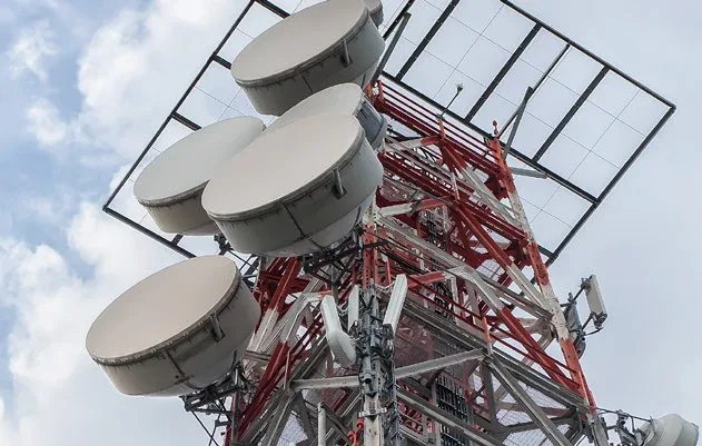
Checkpoint
Trace routing on a PCBA can dramatically affect EMI.
In this context, a well-crafted PCBA must not only curtail its EMI emissions but also demonstrate resilience against high EMI levels. This article will primarily focus on the latter aspect—how to fortify your PCBA design against EMI, ensuring its integrity and optimal performance in challenging electromagnetic environments.
Understanding Electromagnetic Interference
PCBA designs that incorporate every available filter and shielding measure blindly in the hope that something will work are not only ineffective but also expensive. An optimal PCBA design is rarely achieved with a haphazard strategy. To reduce, control, or even eliminate EMI emissions, you need a fundamental understanding of their origins.
In electronic systems, EMI emissions can interfere with normal operation by creating electromagnetic ‘noise’ or disturbances. EMI emissions originate from a variety of sources.
Sources of EMI
One of the primary causes of EMI emissions is common mode currents. Common-mode currents exist at locations where they were never intended and flow in the same direction through multiple conductors like power supply lines, signal cables, or grounding paths. These unwanted parasitic effects can often be attributed to poor routing design. To deal with EMI issues effectively, it’s important to be aware of all the different ways these unintentionally induced currents can occur:

Parasitic capacitance: Capacitance is the ability to store charge, and parasitic capacitance is the unwanted capacitance that occurs in an electronic circuit because of the close proximity of the circuit components. Parasitic capacitance can form an alternate path for the current that has less impedance (or resistance to the flow of current) than the intended path.
We know that when alternating current (AC) flows in an electronic circuit, it generates an alternating magnetic field around it. If another conductive path is nearby (like the unintentional one formed due to parasitic capacitance), this alternating magnetic field can induce an alternating voltage (and hence an alternating current) in that path. This is known as capacitive coupling, or electric field coupling.
This unintentionally induced current can interfere with the normal operation of the circuit, creating noise or disturbances — the essence of Electromagnetic Interference.
Moreover, these unintentionally formed conductive paths (due to parasitic capacitance) can act as antennae, especially at high frequencies, emitting electromagnetic waves into the surrounding space. This is another way in which EMI can be caused: the emitted electromagnetic waves can cause interference in other nearby electronic devices.
In short, parasitic capacitance can enable electric field coupling in a circuit, leading to EMI that can disturb the operation of the circuit itself or other nearby devices.
Parasitic inductance: Parasitic inductance is the unintentional inductance that exists in a circuit due to the physical layout of the circuit components. This unintentional inductance facilitates the process of magnetic field coupling by providing unintended loops through which magnetic field lines can pass, potentially inducing strong currents in nearby conductors and leading to EMI.
As with parasitic capacitance, parasitic inductance effects become more pronounced at higher frequencies, leading to increased EMI potential.
High-speed fast rise time signals: Switching devices, such as transistors, ICs, and digital logic circuits, generate fast rise and fall times, resulting in high-frequency components in their signals. These high-speed signals can radiate electromagnetic energy, especially if not properly controlled.
Emissions from intentional signals: Intentional signals, those necessary for the operation of a circuit, can unexpectedly produce EMI. Let’s consider two main sources: loop-mode emissions and common-mode emissions.
Loop-mode emissions are generated during the normal operation of your circuit. They arise from the electromagnetic fields created by current that flows through the signal traces of your circuit and then returns either through a reference plane or a specifically designed return path.
On the other hand, common-mode emissions occur when the return current flows through a trace positioned near the edge of the reference plane. To reduce the risk of common-mode emissions, one practical design tip is to maintain a safe distance between high-frequency traces and the edge of the PCBA board, ideally at least a half-inch.
- Emissions from unintentional signals: Unintentional signals originate from an intentional signal that has somehow transferred onto a conductor not designed to carry that signal.
This unwanted coupling can lead to EMI. For example, commonmode currents from these signals can create EMI. Similarly, ‘crosstalk,’ where an intentional signal is transferred onto an unintended conductor, for instance, crosstalk coupling between high-speed signal traces and I/O traces can lead to EMI.
Heatsinks: A heatsink, which is usually metal, is placed on top of a high-speed integrated circuit to facilitate cooling. The close proximity allows the IC’s internal currents to unintentionally couple with the heatsink, causing it to act as an antenna. Since these heatsinks are mounted very close to the IC’s high-frequency part, internal currents can easily flow through them.
To manage these emissions, it’s common practice to ground the heatsink to the ground reference of the PCBA board. This grounding reduces the voltage difference between the heatsink and the ground reference plane, thereby minimizing the associated emissions.
Effects of EMI on PCBAs
EMI effects on PCBAs range from minor disturbances in functionality to more severe outcomes, including total system failure. Here’s an overview of potential issues:
- System Performance Degradation: EMI can subtly impact the functionality of PCBAs, causing difficult-to-diagnose intermittent issues. These may include unexpected system behaviors, erratic errors, or slower-than-normal performance. A system failure may not always occur, but it will make the system feel unreliable and frustrating.

- Data Corruption: Electromagnetic disturbances can interfere with the data transmission process, leading to errors in data reading or writing. As a result, data can be corrupted or lost, which has disastrous consequences in systems like medical devices and aerospace electronics.
- Signal Interference: High-frequency EMI, in particular, can interfere with wireless communication signals. If a PCBA is part of a device that relies on wireless communication, EMI can cause dropped signals, decreased signal strength, or increased error rates.
- False triggering: EMI can cause false triggering of sensitive devices. As a result, system functions could be activated unexpectedly.
- Regulatory Compliance Issues: Devices that generate too much EMI can fail to meet regulatory standards, which stipulate limits on the amount of electromagnetic noise a device can emit. In some markets, non-compliance can result in the inability to sell the product.
Design Considerations to Shield PCBA from EMI
EMI is usually confined to specific frequencies, not spread widely across the spectrum. Resonant frequencies in your system will often enhance the EMI’s effect, but resonances aren’t the source of EMI. Instead, they act as loudspeakers that amp up existing EMI, making it more noticeable and problematic.
The best way to deal with EMI effectively is to know your system inside out, including its unintended (‘parasitic’) elements, potential resonances, and how your circuitry is combined. By considering this early in the design process, you’ll be able to save yourself a lot of trouble later in the process. As a result, your system will be more likely to meet EMC standards right away.
Inductance Effects
When dealing with high-frequency signals, inductance is a crucial factor to consider. The reason: When current flows through metal, it creates inductance, resulting in an impedance (resistance to current flow) and a voltage potential. Noise can be introduced across grounding planes, signal strength can decrease, and EMI emissions can rise.
Consider Critical Signals
Your attention should be focused on signals that switch frequently since not every signal on a PCBA contributes significantly to EMI emissions. These signals include clock signals, memory signals, address and data bus signals, data strobe signals, video signals, and any other signal with high speed and wide bandwidth. Pay attention to these signals as they could potentially emit EMI.
Current Radiates and Not Voltage
For matters related to EMI, the current is of primary concern. Always remember the fact that current radiates and not voltage. EMI is primarily caused by the flow of electrical current, not voltage alone. The current generates electromagnetic fields, which radiate and interfere with other devices. While voltage drives the current flow it does not directly produce radiation.
Managing current flow is vital to reduce EMI by minimizing the generation and propagation of electromagnetic fields. Effective circuit design, shielding, and grounding techniques help control current and minimize interference with other electronic systems. It is therefore useful to analyze the currents on a trace as well as the voltage waveforms.
Explicit Design of Return Paths
In many instances, emission sources are closely related to the return current path or absence of it. Board layout design shouldn’t be merely about routing a trace from the driver to the receiver. Instead, it is equally important to take into account the return current signal path. When you consider these factors during the design phase, you can reduce the likelihood of encountering EMI problems during testing or operation.
Tips to Mitigate or Avoid Electromagnetic Interference
You want to create robust, reliable devices that deliver optimal performance, despite potential interference. Here are seven tips that will help you achieve this goal.
Tip 1: Using Shielding Techniques

The first line of defense against electromagnetic interference is shielding. Use metals that absorb or reflect electromagnetic radiation, such as steel, copper, and aluminum.
Shielding methods are available in several forms. The enclosure shielding method involves wrapping your entire device in a conductive casing. The cable shielding method uses shielded cables to shield signals from EMI interference. The last method is board-level shielding, which involves placing small shields around specific components.
Tip 2: Implementing Proper Grounding Strategies
A safe path for dissipating interference is provided by grounding. It can minimize EMI. In order to implement effective grounding, create a single unified ground point to avoid ground loops. Failing to ground properly could lead to EMI accumulation and potentially wreak havoc on your device’s components.
Tip 3: Utilizing Filtering Components
A common practice is to use decoupling capacitors between the power plane and the ground plane on a PCB. These capacitors serve two important functions.
The first benefit of these capacitors is that they maintain the proper functionality and signal integrity, ensuring stable voltage levels and a smooth power supply to the circuit. Furthermore, decoupling capacitors reduce noise injected into the ground-reference plane and power plane pairs. By taking this action, EMI emissions from the edge of your circuit board are significantly reduced, providing an effective method of mitigating EMI in your electronic device.
Tip 4: Pay Attention to Component Placement and Board Layout
EMI is greatly affected by how components are arranged on a PCBA. Critical components should be placed first, based on their orientation and proximity. Components that generate high EMI should be located away from those that are sensitive.
However, placement is just one part of the equation. Thoughtful board routing is another part. By meticulously selecting which layers to route which signals, you can allow return currents to remain near the corresponding signal traces. This careful routing strategy can considerably enhance the EMC performance of your device compared to random routing.
Also, remember to consider the return current path in your design. This often-overlooked aspect is crucial in achieving good EMC performance and minimizing EMI.
Tip 5: Be Strategic with Board and Trace Routing
Your trace routing on a PCBA can dramatically affect EMI. Aim for short and direct traces to minimize EMI risks.
Parallel traces can act as antennas, while perpendicular traces can reduce crosstalk. Consider multilayer boards, where power and ground planes shield traces.
Tip 6: Opt for Differential Signaling When Possible
Differential signaling is a technique for transmitting information that can reduce EMI quite effectively. It transmits two versions of a signal - one is the inverse of the other.
When the receiver compares the difference between these signals, it can accurately reconstruct the original signal. This method is resistant to EMI, as any interference picked up by the transmission line will affect both signals equally, and hence will be canceled out when the difference is taken.
Tip 7: Never Underestimate Regular Testing and Revisions

EMI tests, like radiated emissions testing and conducted emissions testing, can help pinpoint EMI sources in your design.
Schedule these tests throughout the design process, and revise them as necessary to curb EMI. Consistent testing and revisions ensure your design adheres to EMI standards and regulations.
Conclusion
EMI poses a substantial threat to the efficient performance of PCBA designs, affecting system performance and regulatory compliance. Therefore it is crucial to understand the different ways your circuit can produce common-mode currents that cause EMI emissions.
Armed with this knowledge, you can make well-informed trade-offs in your design process. Several design considerations can be used to mitigate EMI, such as shielding techniques, proper grounding strategies, the use of filtering components, strategic component placement, and differential signaling.
By diligently implementing these strategies during the design phase, it’s possible to mitigate EMI issues, save on redesign costs, ensure regulatory compliance, and guarantee the efficient operation of the electronic system.
Related Topics
Struggling with Inflexible PCB Assembly? MacroFab's Got Your Back.
Many electronics designers struggle with systems that demand complete data and specific formats upfront. Wouldn't it be great if there was a better way?
Fab Insights: HASL vs ENIG
Choosing the right surface finish for a PCBA can be tricky. HASL and ENIG differ in their methods of coating printed circuit boards.
How Do QFN Packages Compare to Other Surface Mount ICs?
This article aims to arm electrical engineers and PCBA designers with comprehensive insights into the QFN package.
Download MacroFab’s Engineering Essentials: The PCBA Design Handbook
to learn more about PCBA design basics.
About MacroFab
MacroFab offers comprehensive manufacturing solutions, from your smallest prototyping orders to your largest production needs. Our factory network locations are strategically located across North America, ensuring that we have the flexibility to provide capacity when and where you need it most.
Experience the future of EMS manufacturing with our state-of-the-art technology platform and cutting-edge digital supply chain solutions. At MacroFab, we ensure that your electronics are produced faster, more efficiently, and with fewer logistic problems than ever before.
Take advantage of AI-enabled sourcing opportunities and employ expert teams who are connected through a user-friendly technology platform. Discover how streamlined electronics manufacturing can benefit your business by contacting us today.