In wireless product development, what happens behind the scenes when selecting, designing, and integrating an antenna into a product? What is the journey of a PCB antenna, or more specifically, a PCB-mounted embedded antenna?
Designing and integrating an antenna may seem complex, but it can be broken down into manageable steps. It begins with defining the product’s requirements, which drive the antenna specifications. Next, you select and design the appropriate antenna type. Then, verify the design’s performance through simulations. After building and testing prototypes, manufacturing begins.
Each step demands careful attention. This article offers a clear, step-by-step guide to the PCB antenna design process, explaining each stage and providing practical tips to help you successfully integrate the antenna into your wireless product.
Step 1: Requirements Engineering
If possible, make the prototype from the same materials, using the same manufacturing processes and facilities as the final product. This ensures accurate testing.
The first step in designing an antenna for wireless solutions is to identify and document the product’s essential needs. This process is known as Requirements Engineering (RE).
RE focuses on understanding what needs to be designed, not how. To effectively define these requirements, the design team must conduct a thorough problem analysis. This analysis should address several critical questions to ascertain the operational and environmental conditions under which the product will function. These include:
- What types of communication protocols will the product support (e.g., WiFi, cellular, GPS)?
- What operating frequency and bandwidth are required?
- What are the coverage, gain, and cost expectations?
- Will the product operate indoors, outdoors, or under specific environmental conditions such as extreme temperatures or high humidity?
- How much space can be afforded for antenna clearance on the PCB?
The product requirements define the necessary antenna specifications, which help narrow down the possible antenna technologies. When proposing antenna solutions, include a detailed assessment of the costs, timeline, and, if possible, recommendations for placement and orientation.
Document all antenna and product requirements in a way that supports testing. These requirements should guide the design process and serve as a checklist during testing to ensure the design meets the goals.
Step 2: Design
The design stage starts by using the requirements defined in the RE phase to select the appropriate antenna type and design its specifications to meet those needs.
The antenna must be designed to cover the required frequency and range. Its key parameters, such as efficiency and directionality, should align with the product’s needs. The polarization of both the transmitting and receiving antennas must match to maximize power transfer. The Voltage Standing Wave Ratio (VSWR) should be kept low and the return loss high.
When attaching the antenna to a PCB, match the antenna’s impedance with the characteristic impedance of the feed line connecting it to either a transmitter or a receiver. Impedance mismatches can significantly reduce the RF link budget, lowering the antenna’s efficiency and range.
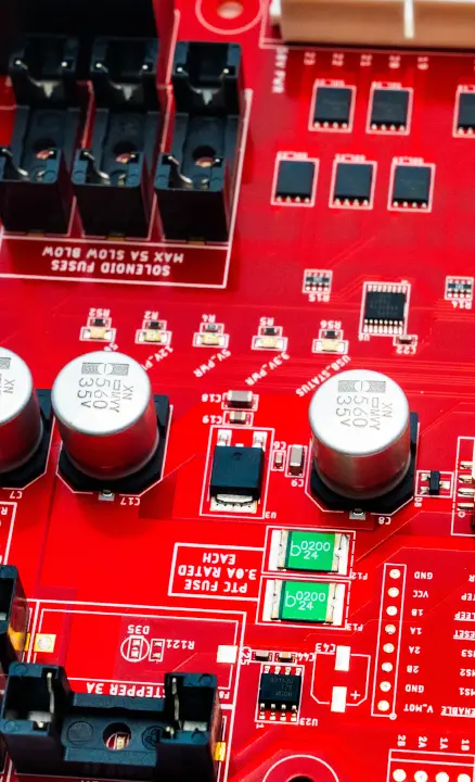
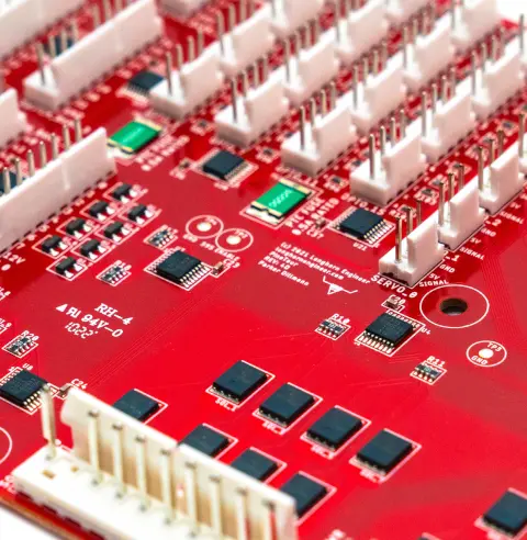
Remember, an antenna is a sensitive component. Its performance is greatly influenced by its placement, surrounding components, the ground plane, and the enclosure or casing.
- Antenna Placement: Antenna placement on the PCB is crucial. Datasheets often suggest various placement options. Choose one of these for optimal performance. If you need to place the antenna elsewhere, you’ll need to validate the placement through careful study.
- Nearby Components: Placing metallic objects near an antenna can interfere with its performance. Metallic objects reflect the antenna’s radiated energy back to the antenna. It’s best to avoid this, or at least account for these components when designing and tuning the antenna. Finalize the device’s mechanical layout before tuning the antenna, as changes later on can disrupt the tuning.
- PCB Size and Ground Clearance: PCB size is crucial for ground-dependent antennas because the board itself affects radiation. Follow ground clearance guidelines in datasheets to avoid poor performance due to detuning or reduced efficiency.
- Casing: Materials used to manufacture the device casing can be critical for the antenna’s performance. This is even more critical for small antennas. If the dielectric material properties are available, it is better to choose a material with low permittivity and dielectric losses that are as low as possible. Such materials are virtually transparent to the antenna’s radiation.
For more in-depth guidance during antenna design, refer to our previous white paper covering six essential considerations for PCB antenna design.
Step 3: RF Simulation
To shorten and ensure reliable design cycles for PCB antennas, designs must be verified early on. However, predicting antenna performance is challenging, as solving Maxwell’s equations requires complex algorithms. Electromagnetic simulators can help predict performance and optimize antenna designs before building physical prototypes.
Remember, however, these simulators are tools, not replacements for the designer. They can predict performance based on the designs you give them, but you need a strong understanding of antenna theory to use them effectively.
Choosing the right simulation method is also important. Popular algorithms include the Method of Moments (MoM), Finite Element Method (FEM), Finite Difference Time Domain (FDTD), and Finite Integration Technique (FIT). Each has specific advantages and disadvantages summarized below:
| Algorithm | Advantages | Limitations |
|---|---|---|
| Method of Moments (MoM) |
|
|
| Finite Element (FEM) |
|
|
| Finite Difference Time Domain (FDTD) |
|
|
| Finite integration technique (FIT) |
|
|
Learn more about the challenges of RF PCBA design now.
Choosing the Right Simulation Method
Selecting the appropriate EM(Electromagnetic) analysis tool depends on factors like ease of model creation, integration with circuit simulation tools, and the level of EM expertise required.
For planar structures, such as PCB interconnects and planar antennas, the MoM is most effective. For fully 3D structures like connectors, packages, and 3D antennas, FEM or FDTD methods are better.
For complex 3D structures with many ports, FEM is ideal. FDTD is best for large structures with fewer ports, such as antenna placements on vehicles or aircraft, and for evaluating antenna performance near detailed human body models.
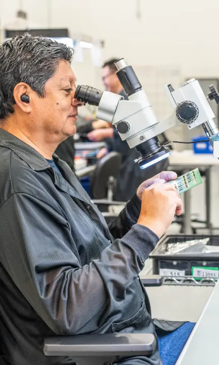
Step 4: Performance Tests and Optimization
After optimizing the designs, prototypes are built for testing. These tests take place in an anechoic chamber designed to absorb all sound waves. Key measurements include return loss, efficiency, maximum gain, Effective Isotropic Radiated Power (EIRP), Total Radiated Power (TRP), Total Isotropic Sensitivity (TIS), and impedance. These measurements fully assess the antenna’s performance. If the results show any issues, the design can be adjusted.
Testing falls into two categories: passive and active.
Passive antenna testing evaluates the antenna alone, without the influence of the rest of the device. The antenna port is isolated from the RF front end and connected to a vector network analyzer (VNA) set to specific frequencies and amplitudes. The VNA measures data, which is then used to calculate efficiency, gain, directivity, and EIRP.
Active antenna testing measures the antenna as part of the entire system, including the RF front end. The main measurements are TRP and TIS.
TRP measures the total power radiated by the antenna when it is transmitting across a frequency band. TIS measures the average sensitivity of the receiving antenna system over a frequency band. TRP and TIS are key indicators of signal quality, offering a reliable gauge of the system’s overall performance.
Practical Considerations During Testing
- If possible, make the prototype from the same materials, using the same manufacturing processes and facilities as the final product. This ensures accurate testing.
- Start critical measurements and prototype testing early. This speeds up the successful production of the final product.
- Antennas must be customized to their specific environment and materials, as they may not perform as expected based on datasheets. Testing should simulate real-world conditions by considering the intended use cases and positions, such as near the head, body, or on different surfaces.
- When planning tests, verify if the product must meet specific regulatory requirements. For instance, for cellular IoT devices, TRP and TIS are crucial, as failing to meet carrier standards for these parameters can prevent product approval.
- Follow regulatory standards for electromagnetic emissions and safety. Include electromagnetic emissions compliance checks throughout the design and testing process. This ensures legal compliance and prevents interference with other devices.
Antenna testing offers significant advantages. It allows designers to optimize the antenna’s design for better radio performance, considering factors like product size, typical use, manufacturing costs, and RF exposure. Even a small improvement, such as a 6 dB gain, can double coverage, while a 3 dB gain can cut the power amplifier’s energy consumption in half, leading to longer battery life. As a result, users experience extended range and enhanced signal quality.
Learn about designing high-frequency PCBAs for distributed antenna systems (DAS) now.
Step 5: Manufacturing
The final step is manufacturing. Success in this stage depends on a stable design, a reliable production process, and effective end-of-line testing. Even the best designs are useless if they can’t be produced efficiently and with high quality. To achieve this, consider the following when selecting and collaborating with a manufacturer:
- Early Collaboration: Involve the manufacturer early in the design process. Close collaboration between design, manufacturing, and materials teams throughout all stages—from design and prototyping to production—ensures a smooth transition to manufacturing, saving time and costs.
- Quality Assurance: Choose a manufacturer that offers robust quality assurance, including innovative end-of-line testing methods. Ensure any overseas facilities comply with local legal standards and maintain strict confidentiality agreements.
- Timely Production: The manufacturer must meet your deadlines and pricing requirements without compromising on quality. Confirm their average lead time to ensure they will deliver on schedule and within budget.
- Fabrication Tolerances: Select a fabrication process capable of meeting tight tolerances. Use prototyping and testing to evaluate the manufacturer’s capabilities and limitations and how their fabrication tolerances impact antenna performance.
Listen to this classic Circuit Break podcast episode to hear about the Wireless Research Center and FCC Pre-Cert Testing.
Conclusion
Designing and manufacturing antennas is a complex process. It is crucial for the success of any wireless product. Choosing the right partner is essential. The design team must work closely together. They need to understand the product’s requirements. They must also follow regulations on frequency, power output, EMC, and testing.
The design should consider factors like PCB size, ground plane, casing, placement, and nearby components. Early design verification is important. Rapid prototyping helps speed up production. Ultimately, even the best designs are only valuable if they can be manufactured efficiently.
Ready to start your PCB Antenna prototype?