What Impedance Control is and how MacroFab Helps You Solve It
Signal fidelity is a key to success in designs employing high speed digital or analog circuits across complex multi-layer printed circuit board (PCB) systems. The transmission line impedance must be accurately maintained across the important signal paths as intended by the design. By working with MacroFab as your PCB partner to identify key traces and sensitive areas of the circuit for matching, the impedance across the system board can be maintained for successful prototyping and manufacturing.
What is Trace Impedance?
Trace impedance is the sum of all the resistance and reactance components of an electrical signal path. An ideal transmission line must have a characteristic impedance that matches both the transmitter and receiver of the intended signal.
If the characteristic impedance of the matched transmission line is faithfully maintained, then the full signal sent by the transmitter is seen by the receiver at the end of the trace. There would be no reflection or attenuation of the signal.
The full amount of signal power is absorbed by the receiver.
For mismatched impedance, a reflection will occur at the far end and the complete signal will not be seen accurately at the receiver destination. Therefore, in practice, the details of the impedance control within the system need to be carefully considered.
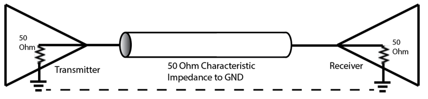
For single-ended line transmission of an I/O signal, a 50 ohm impedance is often the required matching characteristic. The characteristic impedance of the signal path is a continuous 50 ohm path relative to the closest ground. The signal will return on the nearest ground path to the trace. Several applications have specific impedance requirements other than 50 ohms, based on legacy standards. Analog CATV video signals require a 75 ohm single-ended characteristic impedance, for example.
Characteristic Impedance
Real-world parasitic effects and materials that may not be matched cause the ideal transmission line to become a bit more complex. A lack of attention to the design can lead to signal loss and reflections caused by non-idealities in the board layout and assembly.
The characteristic impedance of a trace is determined by the stack-up geometry and PCB materials used within the transmission line. If this is accurately manufactured, the characteristic impedance will be independent of the trace length. This means that a 50 ohm impedance line could be 1mm, 1cm, 1m, or 1 km or more in length.
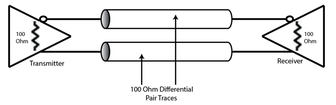
High-speed differential communication signals are not primarily referenced as signal-ended to ground. Instead, a signal pair is used to transmit and receive high-speed digital or RF data. In place of a single-ended specification, maintaining a consistent 100 ohm differential impedance between the + and – signals within the pair is paramount. In this case, while measuring down the + signal of the pair, the trace must maintain close to a 100 ohm impedance relative to the – side of the pair. The tolerance of the 100-ohm requirement across the trace pair is often stated within the IEEE standard, such as USB, HDMI, or JESD204B.
Any unique impedance control considerations that need to be recognized within the design must be communicated using additional files to correctly manufacture your PCBs. The file information will identify the impedance-controlled traces and their resistance, width, and spacing.
An assembly document can show the traces requiring impedance control, provided as either a separate Gerber file or an image with the traces marked. Impedance control requirements are selected at the time of PCB request.
Dielectric PCB Material
The dielectric choice for the board will dictate the signal bandwidth that can be sent down a PCB trace. As signal rates increase for high-speed analog and RF applications, normal FR4 material may not provide adequate bandwidth for the system board.
Exotic dielectric materials can be used for high bandwidth applications instead of standard FR4 material. Check with MacroFab to determine if your selected premium dielectric materials are in stock or need to be ordered for your design. For more information about the physical properties of the PCB material MacroFab uses and stack up information check the knowledge base.
Coplanar Waveguide
A special trace for microwave frequency signals is called a coplanar waveguide.
In a conventional coplanar waveguide, a central conductive strip, typically copper, is printed on a dielectric substrate. Flanking this central strip are two ground conductors, positioned on the same plane as the central strip, hence the term 'coplanar'. These ground conductors are separated from the central strip by a uniform gap, ensuring that they are consistently spaced along the length of the waveguide.
The design extends the ground conductors beyond the length of the central signal conductor to establish a complete ground return path. This configuration is critical for maintaining the integrity of the signal transmitted through the central conductor.
A key aspect of the coplanar waveguide design is the precise control of impedance between the central conductor and the ground conductors. This impedance control is essential for preserving signal integrity, ensuring minimal signal loss and distortion as the signal travels through the waveguide.
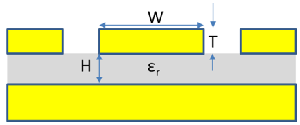
In high-frequency PCB design, the impedance of signal traces is influenced by the circuit's geometry and requires precise calculation. These calculations are complex, involving four key parameters:
Height (H) of the dielectric stack: This is the material layer between the signal trace and the signal return plane. The signal return might be on the same plane as in a coplanar waveguide or on a different plane.
Trace conductor thickness (T): The thickness of the signal trace conductor.
Width (W) of the signal trace conductor: This dimension can vary, especially for outer PCB traces which are often plated, leading to about a 20% uncertainty in their width.
Dielectric constant (Er), or relative permittivity, of the PCB material: This constant quantifies the electrical behavior of the dielectric material and is fixed once the material is chosen. For instance, FR4 typically has an Er of 4.4. Even minor variations in Er can significantly affect the final impedance tolerance. Only specialized materials have precisely defined dielectric constants.
Impedance in traces depends on more than just their size. When designing traces for controlled impedance, maintaining the accuracy of the impedance is more critical than the exact geometry of the layout.
To ensure impedance accuracy, parameters like trace width, height, or dielectric thickness provided in the layout Gerber file may be adjusted by manufacturers like MacroFab. This adjustment ensures that the final impedance falls within the desired tolerance.
PCB Prepregs Materials
Prepregs are semi-cured materials used as bonding materials between two core laminates within a PCB. After the lamination step in the manufacturing process, the final thickness of the prepreg depends on the percentage of copper in adjoining conducting layers, the height of the copper, and the specific type of the prepreg used within the design.
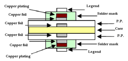
During the lamination process, a high degree of process control and integrity must be maintained. Post-lamination thicknesses of prepregs are reasonably predictable. The resin content of the PCB material is important as the percentage of the resin content has a great impact on the final thickness. The higher the thickness of the dielectric material, the lower the dielectric constant of the PCB material will be.
High-speed materials have lower dielectric constants and are suitable for applications requiring transmission of high-speed signals, usually having signal frequencies above 500 MHz. A layout designer must include the impedance information in the fabrication drawing notes and tables. The information should include the impedance value, the trace width, the spacing for differential pairs and the layer on which the control impedance traces are routed.
For high-speed digital circuits, it is not the signal toggle rate that determines the signal bandwidth. The rise and fall edge times contain the highest frequency components of the signals. In these applications, the bandwidth of the edge rates needs to be computed to properly design for the required dielectric. The bandwidth can be calculated using the measured or required 10-90% rise time of the digital signal. For high-speed GHz signals, we can simplify the equation using the equation below.
BW(GHz) = 0.35/Risetime(nSec)
The width of the trace and height of the dielectric stack-up can be adjusted as needed in order to maintain the tolerance across a signal transmission line for +/- 15% of the ideal impedance value. Achieving this accuracy requires a good understanding of the Er values and experience about how dielectric laminates behave.
PCBA Impedance Classification can be Divided into Three Categories:
No impedance control
In some cases, a circuit design is low-speed and relatively simple. The impedance tolerance is not particularly important and can be loose. No extra precautions need to be taken for the PCB. This is the fastest and least expensive PCB option.
Impedance watching
The circuit designer must identify a particular impedance control trace(s). MacroFab must adjust the width of the trace as well as the height of the dielectric stack. The designer provides final approval on the proposed specifications before any manufacturing starts.
Impedance control
Printed circuit boards with controlled impedance throughout require a meticulous level of accuracy to function correctly. PCB designers must specify the trace impedance and tolerance required. They must work with MacroFab throughout the manufacturing review process to confirm that their specifications are met. These requirements are usually reserved for high-end performance designs or those requiring a very tight tolerance.
Signals that travel across multiple PCB layers using a via will see a change in impedance through the via. The impedance control through a via is harder to manage than through a predefined stack-up.
For the highest sensitive traces, prioritize the routing to maintain signals on a single plane if at all possible. This should include moving transmit and receive components to the top or bottom layers, where the impedance control is the highest. Using internal ground planes between PCB signal layers provides a consistent return signal path and is a good design practice to maintain controlled impedance.
Learn more about high-speed routing design.
Final empirical measurements on PCB test boards can be measured via a Time Domain Reflectometry (TDR) test to determine if impedance specifications are met. Test equipment that measures TDR will send many pulses and observe the responses to show the impedance down the entire transmission line. An open, or unterminated line, will exhibit infinite impedance at the end of the trace.
System impedance control success depends upon planning during the design phase. The design team must identify any critical signal paths and sensitive traces. Those that need to have controlled impedance should be identified early and given special routing priority.
A dielectric material should be chosen that permits the maximum signal integrity, given the bandwidth of the signals within the circuit. The information for the key signals must be communicated and outlined to MacroFab to prepare the design for fabrication. The resulting success of the system will warrant this attention to detail.
Want to know more about impedance? Read How to Optimize PCBA Power Transfer with Parallel Impedance now.
Related Topics
Fab Insights: A Practical Guide to Impedance Control & High-Speed Routing
A discussion on how understanding impedance control can result in successful prototyping and manufacturing when choosing to work with MacroFab.
The 6 Stages of Turnkey PCB Manufacturing
Modern manufacturing partners need to provide more than PCB manufacturing. That’s why the best partners offer turnkey PCB manufacturing in 6 steps.
Ready to get started?
Sign Up TodayAbout MacroFab
MacroFab offers comprehensive manufacturing solutions, from your smallest prototyping orders to your largest production needs. Our factory network locations are strategically located across North America, ensuring that we have the flexibility to provide capacity when and where you need it most.
Experience the future of EMS manufacturing with our state-of-the-art technology platform and cutting-edge digital supply chain solutions. At MacroFab, we ensure that your electronics are produced faster, more efficiently, and with fewer logistic problems than ever before.
Take advantage of AI-enabled sourcing opportunities and employ expert teams who are connected through a user-friendly technology platform. Discover how streamlined electronics manufacturing can benefit your business by contacting us today.