In our previous article, BGA Pad Creation, we spoke about two different styles of pads used for creating BGA (Ball Grid Array) footprints and the benefits of each. BGA components are essential in advanced electronics assembly. At MacroFab, our expertise in BGA assembly, from mid to high volume, meets the diverse needs of clients across Texas, the USA, and the world.
In this post, we discuss methods of routing traces from BGA footprints and how to determine the necessary layer count of your board to ensure reliability in every application.
Definition of Terms
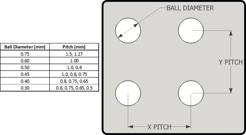
Before we look at laying traces down, there are a few key dimensions that appear on every datasheet for BGA ICs. These dimensions are:
- Ball Diameter – The diameter of the solder ball on the IC
- Pitch – The spacing between two adjacent balls. Typically the pitch is the same in the x and y directions.
These dimensions will determine the properties of our layout, including minimum trace width, via styles, and required layer count.
BGAs come in a variety of ball diameters and pitch configurations. The image below is a chart of typical ball diameters and pitches with a diagram demonstrating the key dimensions.
Example BGA Footprint
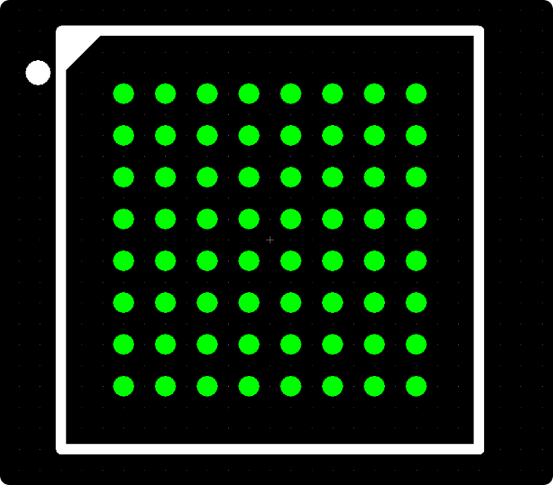
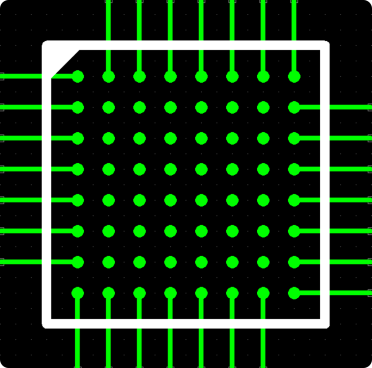
BGA ICs have a wide variety of pin counts ranging from 4 to over 1000 and are typically arranged in an evenly spaced grid of rows and columns. The image below shows an example footprint of a 64 pin BGA arranged in an 8 x 8 pattern with a pitch of 0.8 mm. The nominal ball diameter that should used with this footprint is 0.4 mm. NSMD (Non solder mask defined) pads have been chosen for each landing. NSMD pads are typically defined to be 20% smaller than the ball diameter, so these pads are 0.32 mm in diameter. We’ll use this example footprint below in this post to demonstrate different methods of routing traces.
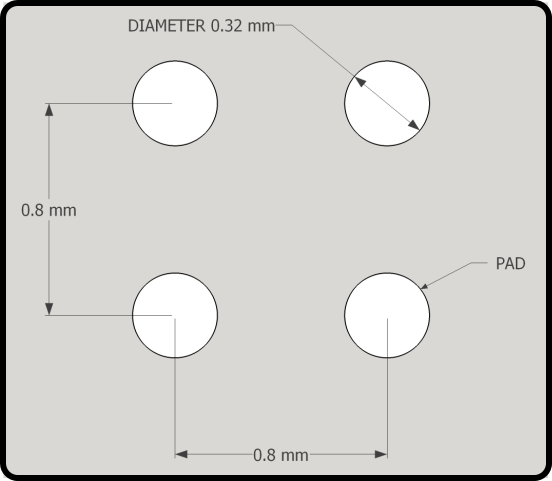
Here is a magnified example of 4 adjacent pads and their dimensions. We will use this magnified view to investigate how to route traces out of the BGA.
Did you know that small solder footprints can lead to bridging and cold solder joints?
Read our solder smoke blog to learn the top 10 causes of magic smoke now.
Signal Layer Count
Because of the high pin count, it’s easy to see that routing traces from each pin out of the footprint is not possible to do on a single layer. Routing traces from pads on the interior of the footprint will require us to utilize multiple signal layers. In most cases, determining how many signal layers are needed for routing a BGA is as simple as counting pairs of rows and columns. For every two rows or columns, an extra signal layer is recommended on the PCB for routing purposes.
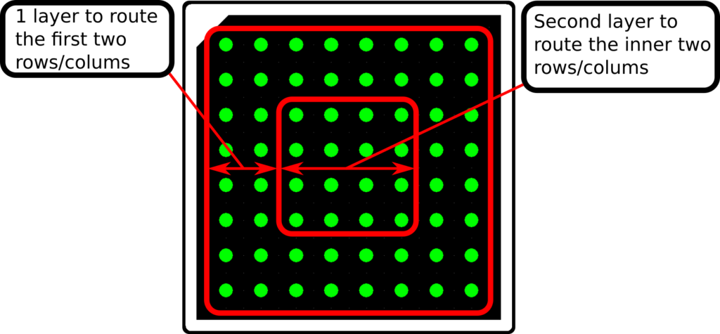
On our example BGA, we can see from the image above that there are two groupings of row/column pairs indicated by the two red squares. The larger square surrounds the first two row/column which will be available to route on a single layer. The smaller red square in the center surrounds the inner pairs of rows/columns, which will require a second layer to route.Larger BGAs with higher ball count will generally require higher layer counts to route.
Routing the Outer Pads
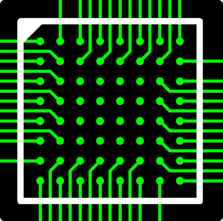
Now that we understand the basic definitions of the footprint, we can begin to route traces from pads. The most obvious place to begin is the outermost row/column since we can simply route traces outward. Below is an image of our example BGA, with the first row routed outward. The trace width was chosen to be 5 mil, and as we will see later, this will not violate clearances and will not increase the cost of manufacturing the PCB due to tight tolerances and small elements.
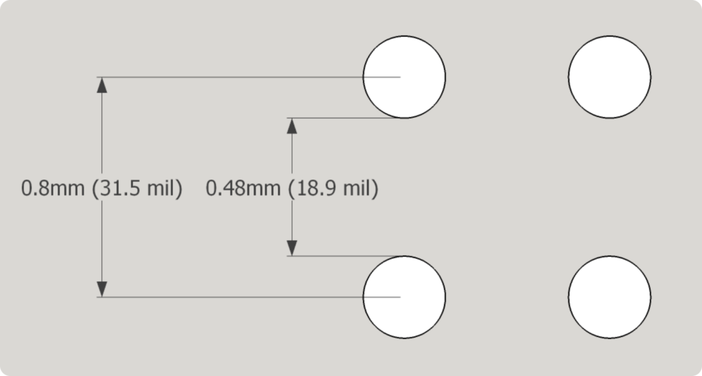
Routing the second layer requires us to place traces in between adjacent pads and traces. Lets start by looking at the space between two adjacent pads. The following image shows the spacing between two adjacent pads.
Calculating the distance between two pads in the x or y direction is as simple as subtracting the diameter of a pad from the pitch.
Spacing between pads = (Pitch – Pad Diameter)
Since the pitch of our example BGA is 0.8mm and the pad diameter is 0.32 (remember we’re using NSMD pads, so the pads are 20% smaller than the ball diameter) the spacing between two pads is 0.48mm or 18.9 mils.
Now that we know the spacing between the two adjacent pads, we can begin to route our traces from the second layer of the example BGA.
By choosing our trace width to be 5 mils, we can see that there is (18.9 mils-5 mil)/2 = 6.95 mils of clearance from the edge of the trace to each pad. A 5.0 mil trace width and 6.0 mils of spacing are standard for PCB manufacturing.
Learn how to pick the right PCB trace width now.
The following image shows the trace spacing / trace clearance in more detail.
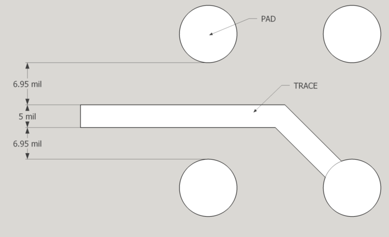
Passing a Trace Between two Pads
Routing the Inner Pads
Now that we have the two outer rows/columns of pads routed, we can focus on the inner pads. Since all of the available paths out of the BGA were consumed by the first two rows/columns of pads, we will have to use another layer on our PCB to route the trace out.
The method most used for routing inner pads is to place a via at the center of 4 adjacent pads, such that a trace from one of the pads can pass to another signal or plane layer on the PCB and then route outward. This method is called “dog bone” since the pad-trace-via connection looks similar to a cartoon dog bone.
Routing inner traces through vias requires more attention to detail as there are more elements to consider. Lets take a look at our zoomed-in drawing to see the dimensions we need to identify. For clarity, the upper right pad has been removed from the image below to show more detail.
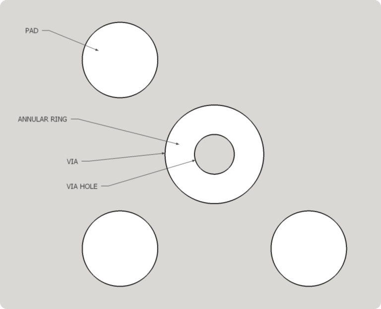
This image shows a via placed at the center of a group of pads. Vias are defined by the hole diameter and the width of the annular ring. We will need to carefully choose a via that will fit between our pads while not violating any clearances. To do this we must find the diagonal distance between two pads. This is easily found by using Pythagoras’ theorem (remember that equation from grade school?) to find the length of the hypotenuse of a triangle formed by the x and y pitch.
To clarify, here is an image showing the dimensions we are trying to find. The dimension H will be calculated from the x and y pitch.
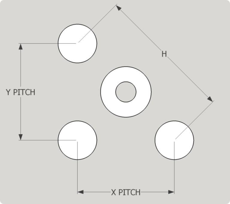
Using Pythagoras’ theorem:
So now that we know the diagonal distance between two pads we can begin to make decisions on how to select an appropriate via. The following image details the important dimensions we need to consider for our via selection.
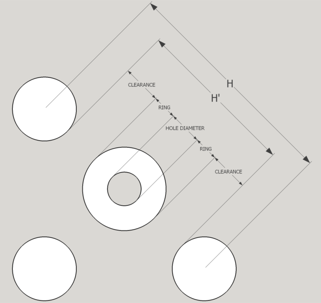
Similar to the previous section where we considered the spacing between two balls, we need to subtract the diameter of one pad from our calculated H. We will call this new dimension H prime or H’. Since our calculated value for H was 1.13 mm, H’ will be 1.13 mm – 0.32 mm = 0.81 mm or 31.9 mils. Now that we have our H’ number, the hole diameter plus our annular ring and clearances must fit within 31.9 mils.
We have already mentioned that the standard manufacturing value for clearances is 6 mils, so we will use that value and subtract 12 mils from our H’ (we subtract twice the clearance value since there is clearance on both sides of the via). This leaves us with 31.9 – 12 = 19.9 mils for the total diameter of the via.
Standard manufacturing values for annular rings are also 6 mils so we can subtract the annular ring from our remaining 19.9 mils to find an acceptable drill size. In this case we end up with 19.9 mils – 12 mils = 7.9mils. It’s probably a good idea to go with a drill that is slightly less than this value so we can design in a little room for tolerance variations. For this example we chose a 6 mil drill.
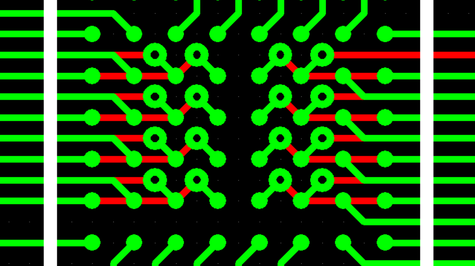
Now that we have our vias defined as having a 6 mil drill and a 6 mil annular ring, routing the inner pads becomes simple. For each pad that needs to be routed out of the footprint, we place a via at the center of a group of 4 pads and connect our trace to it. Once we are connected to our trace, we can route away from the BGA on a layer separate from the one we used on the outer pads.
Above is an image of our example BGA with each pad routed out using dog bones to have the inner traces drop through the via to a second layer.
Connecting to Power and Ground
In the example BGA above, we routed the BGA such that every pad has a trace exiting the footprint. In practice, this would rarely be the case since many pins will be connecting to power and ground. These power and ground pins are typically located near the center of the package which is done to make routing signals easier. In most cases, BGA components will be used on PCBs that have 4 or more layers. Two of these layers are typically dedicated to be ground and power layers. In these situations, the pads that are to be connected to power or ground can be routed using the dog bone method with the via connected directly to the power or ground plane.
MacroFab can build your 4 layer PCB boards and much more. Find out more now.
Wrap Up
By using a few simple rules, we have seen that routing BGA ICs is not a very difficult task. Employing NSMD style pads and dogbone routing allows us to use even the most densely packed ICs. Hopefully the information presented here will equip you to use BGA ICs in your future designs.
Ready to Get Started?