When constructing a footprint for BGA-style components, choosing between solder mask-defined (SMD) and non-solder mask-defined (NSMD) pads is imperative. The correct pad design can mitigate many manufacturing problems and reduce time spent analyzing failures. This article outlines a few simple principles to guide you in creating the right footprints for BGA components.
Understanding SMD and NSMD Pads
There are two basic forms of pads implemented for BGA footprints. One is the Solder Mask Defined pad (SMD) and the other, is the Non-Solder Mask Defined pad (NSMD). Let’s take a look at these two types and discuss how to use them in your BGA designs.
In electronics, “SMD” can also refer to a surface mount device, but in this case we are using it in a different context.
Define SMD (Solder Mask Defined):
* Definition: In SMD pads, a layer of solder mask covers a portion of the underlying copper pad, creating a smaller solder mask opening. * Benefits: * Enables precise soldering due to the reduced copper pad size. * Enhances the overall reliability and performance of the final device. * The solder mask opening acts as a guide during BGA ball placement for solderingDefine NSMD (Non-Solder Mask Defined):
* Definition: NSMD pads differ by leaving a gap between the copper pad and the solder mask, exposing the entire pad. * Benefits: * Offers superior solder adhesion due to full pad contact with the solder ball. * Allows for a smaller pad size, simplifying trace routing, especially for high-density BGAs.Solder Mask Defined BGA Pads (SMD)
In SMD pads, the solder mask aperture is outlined to be smaller than the diameter of the pad that it encompasses. This approach limits the size of the copper pad that the component is soldered to, providing two key benefits.
- Enhanced Pad Security: The solder mask overlay strengthens the connection between the pad and the circuit board. This helps prevent the pad from lifting off (delamination) due to thermal or mechanical stress that the PCB might experience during operation or manufacturing.
- Solder Ball Alignment: The opening in the solder mask acts as a guide, ensuring proper BGA ball placement during the soldering process. This contributes to precise soldering and overall joint integrity.
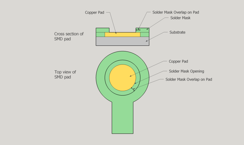
In the top-down view, we can see that the solder mask is specified to cover a portion of the copper pad underneath. Defining pads this way creates two distinct advantages. First, the overlapping mask helps prevent the pads from lifting off of the PCB due to thermal or mechanical stress. Second, the opening in the mask creates a channel for each ball on the BGA to align with while the component progresses through the soldering process.
The copper layer of an SMD BGA pad typically has a diameter equal to the diameter of the pad on the BGA itself. To create the SMD overlay, a reduction of 20 percent is typically used.
NSMD Pads for BGA Components
In contrast, NSMD pads are structured differently from SMD pads. With NSMD pads, the solder mask is designed to not interact with the copper pad, leaving a gap between the pad’s edge and the solder mask. Instead, the mask is created such that a gap is created between the edge of the pad and the solder mask. The following image shows a top and cross-section view of an NSMD-style pad.
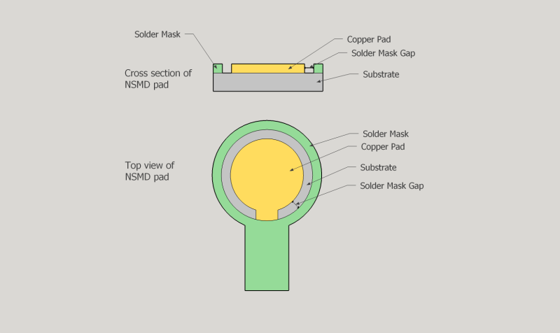
In this method, the size of the copper landing pad is not defined by the mask layer, but only by the diameter of the copper pad itself. NSMD pads can be smaller than the diameter of the solder ball. Typically, this reduction in pad size is 20% smaller than the ball diameter. Since the pad size is reduced with this approach, the additional room between adjacent pads allows for easier trace routing. This can almost become a necessity when routing high-density, fine-pitch BGA chips.
By allowing for a smaller pad size, NSMD pads facilitate easier trace routing - an almost necessary feature when dealing with high-density, fine-pitch BGA chips. However, NSMD pads are prone to delamination from the PCB under mechanical and thermal stress. Following standard manufacturing and handling practices should prevent this from occurring.
Listen to this classic Circuit Break episode when Stephen and Parker dive into the nuances of working with a CM, including reflow profile considerations, solder specs, and BGAs.
Solderability of SMD vs NSMD BGA Pads
The following images show examples (highly exaggerated) of how a solder ball adheres to each style of pad:
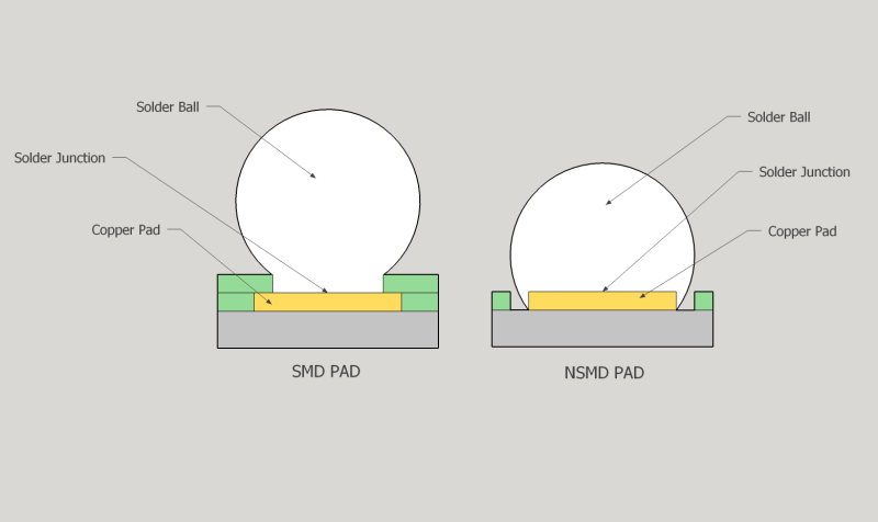
With the entire pad exposed, NSMD pads tend to have better solder adhesion than SMD pads. The solder ball is able to make a connection to the entire NSMD pad instead of the mask-defined portion of SMD pads.
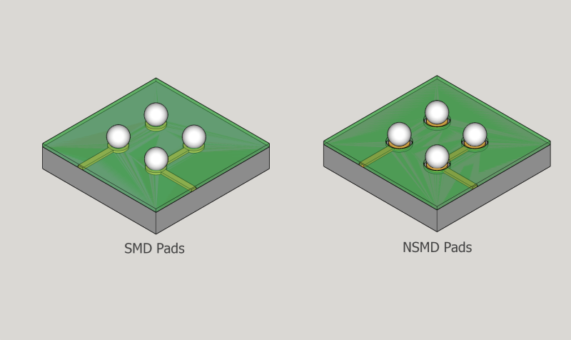
SMD vs NSMD: Which BGA Pad Style to Use
It is important to note that component manufacturers typically provide recommended footprints in the datasheets for their components. When these footprints are available, it’s certainly advisable to use them.
In general, use the NSMD pad style wherever possible due to its improved solderability and pad accuracy. Visit our Knowledge Base for more information.
Going Forward
In the next blog post, we will use NSMD pads to explore how to properly design and route a BGA footprint on a PCB.
Ready to start your next project?