Updated Oct 2024
In our previous series, Programming for PCB Production, we provided an overview of different methods to program PCB products. This article goes into greater detail on one of those methods – how to design and build a programming fixture or jig.
Identifying the Need for a Programming Fixture
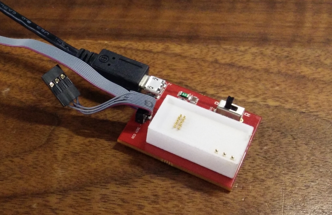
This fixture is designed for products built on a development board that does not have an integrated programming header. See Figure 1 for the development board. The programming fixture will need to power the board and make a connection to the programmer, which in this case is an Atmel ICE programmer and is programmed with the SWD protocol. Figure 2 shows the completed programming fixture.
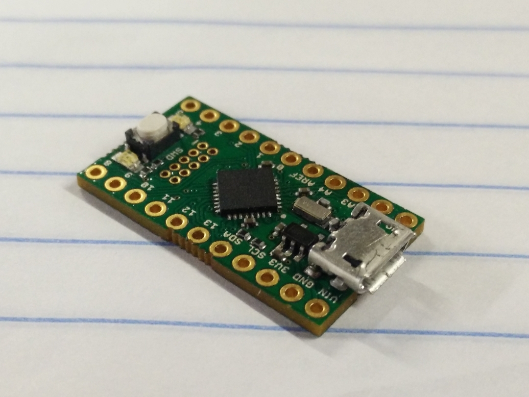
Figure 1: The board that needs to be programmed. Note that there is no programming header.
Designing the Fixture
Figure 2: The completed programming fixture.
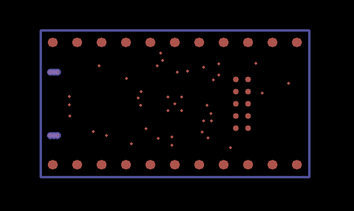
First, I took the design files for the development board and opened them in gerbv. I only used the border file and the drill file (Figure 3). By doing this, I was able to get the precise dimensions of where the pins were in relation to the edge of the PCB.
Choosing the Right Pogo Pins
Figure 3: Development board drill files.
To connect to these pins, I need pogo pins to make contact with the pads. I chose two different pogo pins. Part number 0908-4-15-20-75-14-11-0 was used to contact the power input pins and part number 100803-011 was used to contact the 2×5 50 mil programming header. These parts are roughly the same height, so they can work together. The 100803-011 pogo pins are small in diameter so they fit the 50 mil pitch on the programming header, but they have a large enough head to not poke through the PTH holes on the programming header.
Using the dimensions of where the pins are located and the pogo pin parts, I designed a PCB that connects the Atmel ICE programmer SWD connector to the 100803-011 pogo pins and applied power over 0908-4-15-20-75-14-11-0 pogo pins. See Figure 4 and Figure 5 for the schematic and layout.
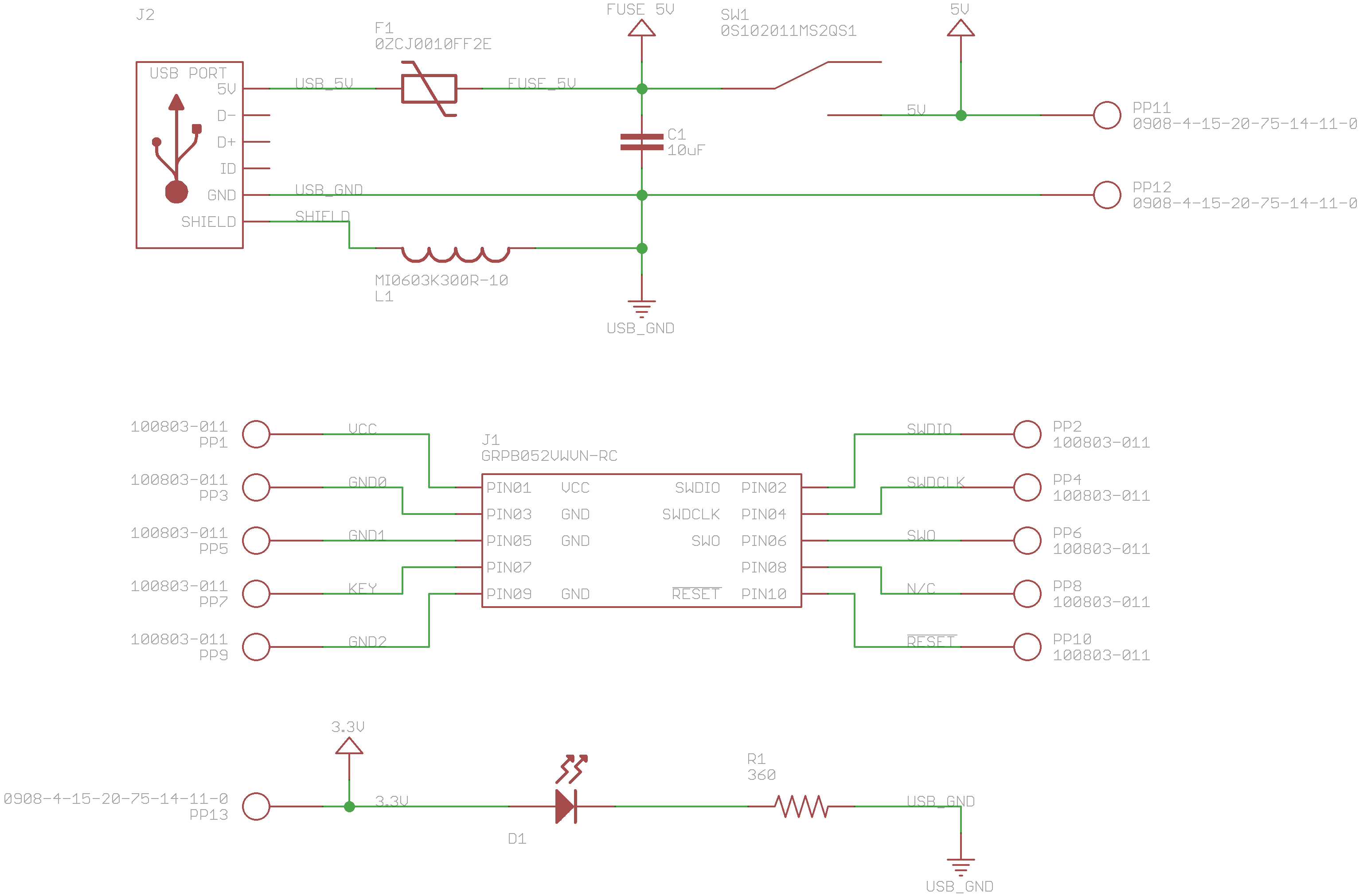
Figure 4: Schematic of the programming fixture.
Creating the Schematic and Layout
Figure 5: PCB layout of the programming fixture.
I decided the easiest way to provide power was over USB. I put an inline 0.25A PTC fuse to prevent a short circuit from destroying the USB port. You can download the Eagle files for the programming fixture here.
To locate the development board onto the pogo pins I designed a 3D printed holder that attaches to the fixture PCB. This holder also prevents side loading on the pogo pins to prevent them from jamming.
Using 3D Modeling Software
Next, I exported the layout from Eagle to a .DXF file and imported that .DXF file into SketchUP. There are a few plugins that will do this for you. This process ensured that my 3D printed holder would line up with the holes on the PCB (Figure 6).
Figure 6: DXF import from Eagle to SketchUp
I made the spot where the development board sits 0.5mm larger then the actual board. This will take care of any tolerance issues with the board routing. The development board sits 6.6mm from the fixture PCB. This number is derived from the 0908-4-15-20-75-14-11-0 pogo pin datasheet. The pogo pin is 8.5mm tall with a 1.4mm stroke on the pin. Since the pad the pogo pin is contacting is PTH we have to take account the round top which would roughly be 0.5mm in radius. This gives us a height of 6.6mm. The 3D file for the holder can be downloaded here. The notch at the end allows the USB connector to overhang.
Figure 7: 3D Printed holder designed in SketchUp. Ready for printing!
Printing the Holder and Assembling the Pogo Fixture
I printed this holder at Shapeways. The 50 mil connector’s pogo pin holes were to small to be printed using my FDM 3D printer. The fixtures PCB was assembled here at MacroFab. Once all the parts arrived I assembled the plastic holder on top of the fixture’s PCB and used super glue to make sure it would all stay together. The completed programming fixture can be seen in Figure 8 and Figure 9.
Figure 8: The programming fixture is complete!
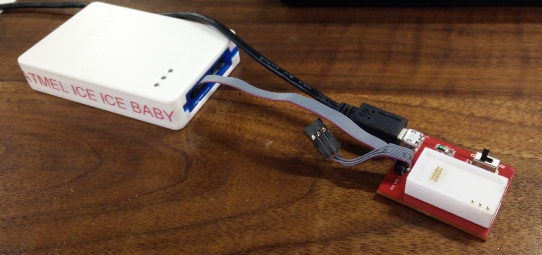
Figure 9: The programming fixture is connected to the Atmel ICE programmer and powered via a micro USB cable.
Operating the programming fixture is very straight forward. The Atmel ICE programmer and a micro USB cable are plugged into the programming fixture. A development board is held onto the plastic holder. The power switch is turned on. A programming routine in Atmel Studio is run which programs the development board. After completion of this routine, the board is powered off and the development board is removed. See Figure 10.
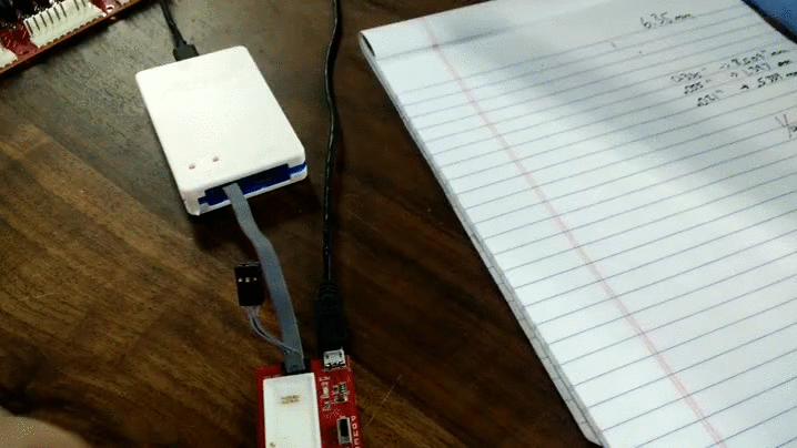
Figure 10: Using the Programming Fixture.