Related Topics
Platform Updates from Kyle McLeod and Nicholas Lundgaard
The episode provides insights into MacroFab's efforts to make PCB manufacturing more accessible and efficient for their customers.
Tracing a Path for PCB Design Automation with Sergiy Nesterenko
Sergiy Nestorenko, founder of Quilter and former SpaceX engineer, discusses revolutionizing PCB design automation.
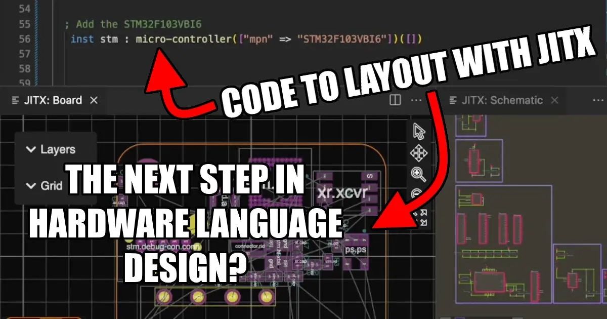
Dr. Duncan Haldane from JITX on Automating Circuit Design
Dr. Haldane on his background, the problems JITX is trying to resolve, & new auto-router plans. What's the deal with the "hyper-aggressive pogo-stick"?
Other Resources
Circuit Break Podcast
Webinars
Videos
Tour MacroFab's ITAR-Compliant Facility
August 4, 2021, Episode #288
PCB design rules for clearances
- Stephen’s favorite calculator
- Clearance and creepage
- According to the IEC (international electrotechnical commission) a global standards organization
- Clearance – The shortest path between two conductive parts, or between a conductive part and the bounding surface of the equipment, measured through air
- Creepage – The shortest path between two conductive parts, or between a conductive part and the bounding surface of the equipment, measured along the surface of the insulation
- IEC/UL 60950-1 Safety standards – has more in depth information on spacing and how to handle mains
- IPC2221 generic pcb design rules – Has simple information on spacing vs voltage
- The creepage requirements depend on
- insulation material group
- Comparative Tracking Index (CTI) is used to measure the electrical breakdown (tracking) properties of an insulating material. Tracking is an electrical breakdown on the surface of an insulating material wherein an initial exposure to electrical arcing heat carbonizes the material. The carbonized areas are more conductive than the pristine insulator, increasing current flow, resulting in increased heat generation, and eventually the insulation becomes completely conductive.
- I 600V
- II 400 to 600V
- IIIa 175 to 400V
- IIIb 100 to 175V
- Comparative Tracking Index (CTI) is used to measure the electrical breakdown (tracking) properties of an insulating material. Tracking is an electrical breakdown on the surface of an insulating material wherein an initial exposure to electrical arcing heat carbonizes the material. The carbonized areas are more conductive than the pristine insulator, increasing current flow, resulting in increased heat generation, and eventually the insulation becomes completely conductive.
- pollution degree
- Degree 1 – no pollution
- Degree 2 – non-conductive contamination that might temporarily become conductive due to condensation
- Degree 3 applies to conductive pollution, or to dry non-conductive one which could become conductive due to condensation
- working voltage
- Altitude and elevation – Multiply by 1.48
- Appliance insulation class
- Functional
- Basic
- Supplementary
- Double Insulation – Double the creepage
- Reinforced – Double the creepage
- insulation material group
- IPC2221 requirements – Actually tend to be larger
- External
- Internal
- Coated
Stephen’s thoughts on the AND!XOR hardware puzzle
About the Hosts

Parker Dillmann
Parker is an Electrical Engineer with backgrounds in Embedded System Design and Digital Signal Processing. He got his start in 2005 by hacking Nintendo consoles into portable gaming units. The following year he designed and produced an Atari 2600 video mod to allow the Atari to display a crisp, RF fuzz free picture on newer TVs. Over a thousand Atari video mods where produced by Parker from 2006 to 2011 and the mod is still made by other enthusiasts in the Atari community.
In 2006, Parker enrolled at The University of Texas at Austin as a Petroleum Engineer. After realizing electronics was his passion he switched majors in 2007 to Electrical and Computer Engineering. Following his previous background in making the Atari 2600 video mod, Parker decided to take more board layout classes and circuit design classes. Other areas of study include robotics, microcontroller theory and design, FPGA development with VHDL and Verilog, and image and signal processing with DSPs. In 2010, Parker won a Ti sponsored Launchpad programming and design contest that was held by the IEEE CS chapter at the University. Parker graduated with a BS in Electrical and Computer Engineering in the Spring of 2012.
In the Summer of 2012, Parker was hired on as an Electrical Engineer at Dynamic Perception to design and prototype new electronic products. Here, Parker learned about full product development cycles and honed his board layout skills. Seeing the difficulties in managing operations and FCC/CE compliance testing, Parker thought there had to be a better way for small electronic companies to get their product out in customer's hands.
Parker also runs the blog, longhornengineer.com, where he posts his personal projects, technical guides, and appnotes about board layout design and components.

Stephen Kraig
Stephen Kraig is a component engineer working in the aerospace industry. He has applied his electrical engineering knowledge in a variety of contexts previously, including oil and gas, contract manufacturing, audio electronic repair, and synthesizer design. A graduate of Texas A&M, Stephen has lived his adult life in the Houston, TX, and Denver, CO, areas.
Stephen has never said no to a project. From building guitar amps (starting when he was 17) to designing and building his own CNC table to fine-tuning the mineral composition of the water he uses to brew beer, he thrives on testing, experimentation, and problem-solving. Tune into the podcast to learn more about the wacky stuff Stephen gets up to.
Special thanks to whixr over at Tymkrs for the intro and outro!
Related Podcasts
Dr. Duncan Haldane from JITX on Automating Circuit Design
Dr. Haldane on his background, the problems JITX is trying to resolve, & new auto-router plans. What's the deal with the "hyper-aggressive pogo-stick"?
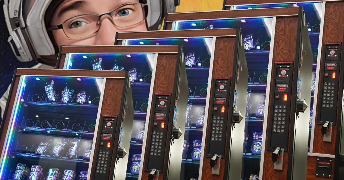
Recursive Vending Machines
Join us as we chat with Hyr0n and Zapp from AND!XOR Group about their iconic badges for DEF CON 31.
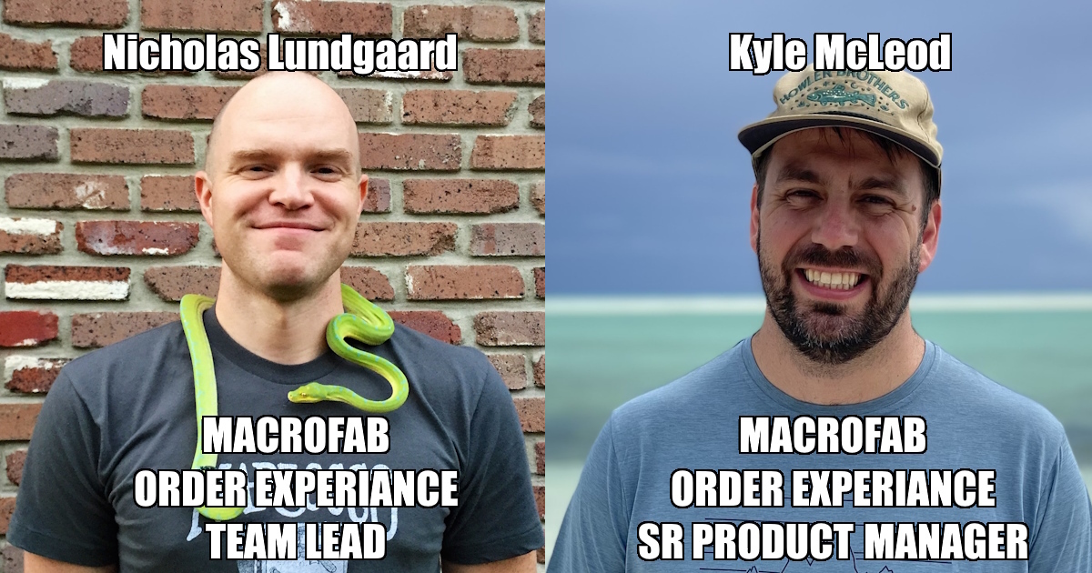
Platform Updates from Kyle McLeod and Nicholas Lundgaard
The episode provides insights into MacroFab's efforts to make PCB manufacturing more accessible and efficient for their customers.
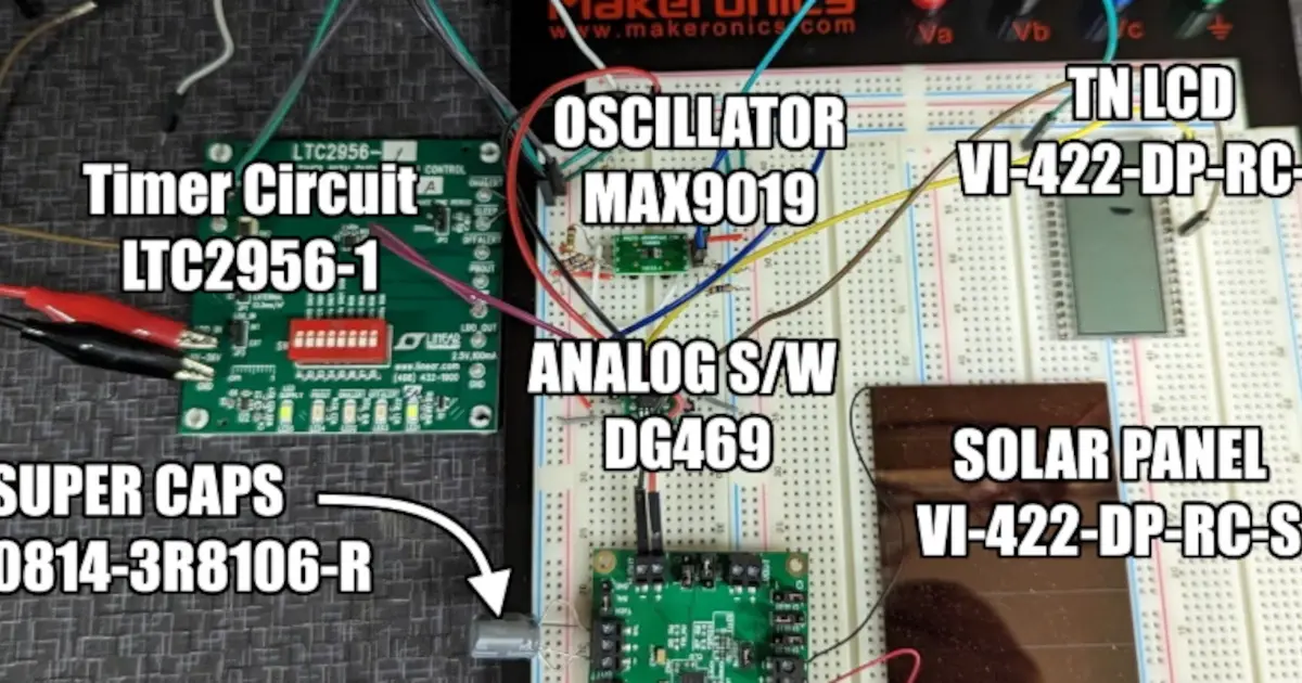
Breadboarding for Success
This week we are talking about Breadboards. Is breadboarding a circuit or design still applicable in today's SMT component dominated world?
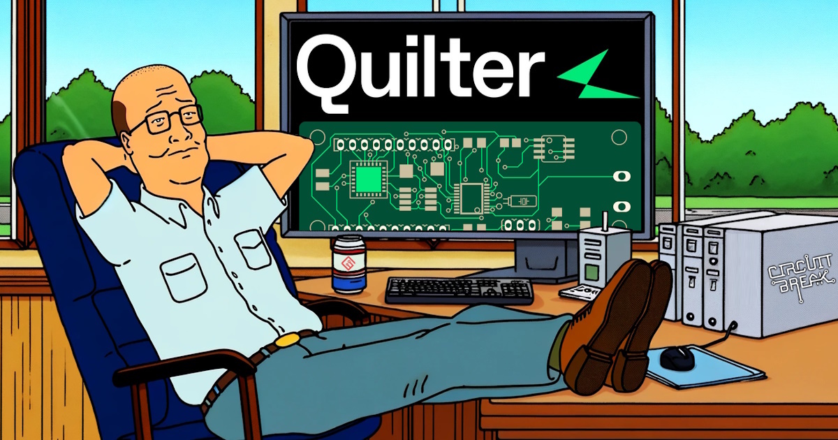
Tracing a Path for PCB Design Automation with Sergiy Nesterenko
Sergiy Nestorenko, founder of Quilter and former SpaceX engineer, discusses revolutionizing PCB design automation.
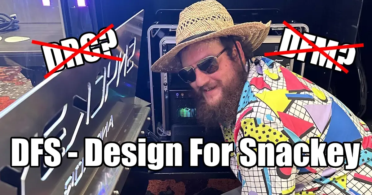
DFS: Design for Snackey
This special episode is recorded at DEF CON, the annual hacker community gathering in Las Vegas.
About MacroFab
MacroFab offers comprehensive manufacturing solutions, from your smallest prototyping orders to your largest production needs. Our factory network locations are strategically located across North America, ensuring that we have the flexibility to provide capacity when and where you need it most.
Experience the future of EMS manufacturing with our state-of-the-art technology platform and cutting-edge digital supply chain solutions. At MacroFab, we ensure that your electronics are produced faster, more efficiently, and with fewer logistic problems than ever before.
Take advantage of AI-enabled sourcing opportunities and employ expert teams who are connected through a user-friendly technology platform. Discover how streamlined electronics manufacturing can benefit your business by contacting us today.