Related Topics
System-in-Package (SiP) Platforms with Greg Sheridan
This week Stephen and Parker discuss System-in-Package (SiP style chips) with Greg Sheridan of Octavo Systems.
Other Resources
Circuit Break Podcast
Webinars
Videos
Tour MacroFab's ITAR-Compliant Facility
October 24, 2018, Episode #143
Podcast Notes
- Gene Frantz – Chief Technology Officer for Octavo Systems
- One of the founders and the visionary behind Octavo Systems
- Professor in the Practice at Rice University in the Electrical and Computer Engineering Department
- Was the Principal Technology Fellow at Texas Instruments where he built a career finding new opportunities and building new businesses to leverage TI’s DSP technology
- Holds 48 patents and has written over 100 papers/articles and presents at conferences around the globe
- Has a BSEE from the University of Central Florida, a MSEE from Southern Methodist University, and a MBA from Texas Tech University
- Erik Welsh – Applications and Systems Manager for Octavo Systems
- Has over 16 years of industry experience designing hardware and software systems, including 11 years at Texas Instruments
- Supported hundreds of developers bringing embedded systems quickly to market
- Simplifying complex systems is a passion and mentors engineers developing embedded Linux systems
- Developed platforms for cutting-edge wireless research to provide open-access to startups
- Began his career as a SoC (System-On-Chip) designer eventually leading SoC Security Architecture development
- Currently holds multiple patents in the area of System-in-Package technology
- Has a Bachelor of Science and Masters in Electrical Engineering from Rice University
- Octavo Systems
- For more background on Octavo Systems check out MEP EP#17: System-in-Package (SiP) Platforms with Greg Sheridan.
- Octavo’s goal is to make designing electronics easier and more accessible with System-in-Package devices that abstract away the tedious complexities that go along with designing an electronic system.
- Ease of use is in everything Octavo does from choosing silicon partners to the way boards are designed. Octavo offers an entire experience to help designers get from an idea to an actual product.
- They offerApplication Notes, a complete tutorial series which walks through setting up Eagle all the way through booting Linux on a custom board, and direct access to system experts through support and forums.
- Severalreference designsare available with more coming.
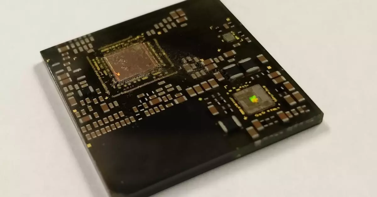
- The new OSD335x C-SiPis a great example. As a Complete System in Package, designers can add a few resistors and power giving a complete Computer in a 27mm package.
- Utilizing System-in-Package not only reduces board BOM but also manufacturing cost at the board level.
- How do System-In-Package devices make designers and engineers lives easier?
- Certification for FCC and CE? Some modules are pre FCC certified with an ID. Is there a benefit using a System-in-Package to reduce product development risk here?
- OSD335x C-SIP
Visit our Slack Channel and join the conversation in between episodes and please review us, wherever you listen (PodcastAddict, iTunes). It helps this show stay visible and helps new listeners find us.

Gene Frantz

Erik Welsh
About the Hosts

Parker Dillmann
Parker is an Electrical Engineer with backgrounds in Embedded System Design and Digital Signal Processing. He got his start in 2005 by hacking Nintendo consoles into portable gaming units. The following year he designed and produced an Atari 2600 video mod to allow the Atari to display a crisp, RF fuzz free picture on newer TVs. Over a thousand Atari video mods where produced by Parker from 2006 to 2011 and the mod is still made by other enthusiasts in the Atari community.
In 2006, Parker enrolled at The University of Texas at Austin as a Petroleum Engineer. After realizing electronics was his passion he switched majors in 2007 to Electrical and Computer Engineering. Following his previous background in making the Atari 2600 video mod, Parker decided to take more board layout classes and circuit design classes. Other areas of study include robotics, microcontroller theory and design, FPGA development with VHDL and Verilog, and image and signal processing with DSPs. In 2010, Parker won a Ti sponsored Launchpad programming and design contest that was held by the IEEE CS chapter at the University. Parker graduated with a BS in Electrical and Computer Engineering in the Spring of 2012.
In the Summer of 2012, Parker was hired on as an Electrical Engineer at Dynamic Perception to design and prototype new electronic products. Here, Parker learned about full product development cycles and honed his board layout skills. Seeing the difficulties in managing operations and FCC/CE compliance testing, Parker thought there had to be a better way for small electronic companies to get their product out in customer's hands.
Parker also runs the blog, longhornengineer.com, where he posts his personal projects, technical guides, and appnotes about board layout design and components.

Stephen Kraig
Stephen Kraig is a component engineer working in the aerospace industry. He has applied his electrical engineering knowledge in a variety of contexts previously, including oil and gas, contract manufacturing, audio electronic repair, and synthesizer design. A graduate of Texas A&M, Stephen has lived his adult life in the Houston, TX, and Denver, CO, areas.
Stephen has never said no to a project. From building guitar amps (starting when he was 17) to designing and building his own CNC table to fine-tuning the mineral composition of the water he uses to brew beer, he thrives on testing, experimentation, and problem-solving. Tune into the podcast to learn more about the wacky stuff Stephen gets up to.
Special thanks to whixr over at Tymkrs for the intro and outro!
Related Podcasts
System-in-Package (SiP) Platforms with Greg Sheridan
This week Stephen and Parker discuss System-in-Package (SiP style chips) with Greg Sheridan of Octavo Systems.
About MacroFab
MacroFab offers comprehensive manufacturing solutions, from your smallest prototyping orders to your largest production needs. Our factory network locations are strategically located across North America, ensuring that we have the flexibility to provide capacity when and where you need it most.
Experience the future of EMS manufacturing with our state-of-the-art technology platform and cutting-edge digital supply chain solutions. At MacroFab, we ensure that your electronics are produced faster, more efficiently, and with fewer logistic problems than ever before.
Take advantage of AI-enabled sourcing opportunities and employ expert teams who are connected through a user-friendly technology platform. Discover how streamlined electronics manufacturing can benefit your business by contacting us today.