MacroFab Resource Download

Real-World RF PCBA Design: Tips and Techniques for Engineers
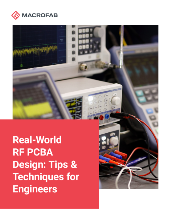
Real-World RF PCBA Design: Tips and Techniques for Engineers

Real-World RF PCBA Design

RF PCBAs are used in many industries, from telecommunications infrastructure to the smartphones in your pocket. Signal integrity is one of the main challenges faced by RF PCBA designs.

This article will discuss the common factors that degrade SI in PCBA designs and outlined key design guidelines. These guidelines span from component selection and placement to PCB layering and routing, designing transmission lines, and implementing effective shielding.

Be sure to also download our companion document: 21 RF PCBA Design Tricks

Register to Download

To download this document, please complete the form below.

* = Required Field
Please enter your first name.
Please enter your last name.
Please enter your business email address.
Please enter your company name.

You can unsubscribe from these communications at any time. For more information on how to unsubscribe, our privacy practices, and how we are committed to protecting and respecting your privacy, please review our Privacy Policy.

Related Resources

Reshaping robotics how pcba advances drive tomorrows autonomous solutions 01

Reshaping Robotics: How PCBA Advances Drive Tomorrow’s Autonomous Solutions

This paper looks at what’s causing the growth in robotics, including its impact on jobs around the world

21 ref pcba design tricks

21 RF PCBA Design Tricks

Download this tip sheet containing 21 tricks for RF PCBA designs.

Executives guide to pcba intellectual property

The Executive's Guide to PCBA Intellectual Property

What you don't know can hurt you. Protect your PCB intellectual property with these tips.