Why PCBA Design Reuse is Becoming More Common
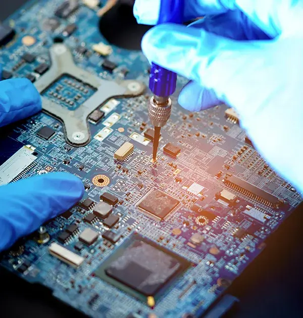
Reusing established designs and concepts is standard practice in some industries, but not in others. For example, the automobile industry has been creating product lines out of a single basic design for decades. Mobile phone developers slightly tweak and add features to the cellphone design and release a new iteration every year.
This concept also extends beyond technology. For instance, housing developers mass-produce homes using a common layout, while clothing designers employ templates for apparel in various colors and materials.
In the context of PCBA manufacturing, design reuse is simply implementing established circuitry and designs in product development. This practice allows developers to utilize proven electrical circuits and PCBA layouts repeatedly, rather than starting from scratch with each new project. While this may sound like a no-brainer, PCBA development is still catching up to other industries when it comes to reusing proven design concepts.
In this blog we’ll look at the potential benefits of design reuse, what’s holding it back in the PCBA arena, and what the future might look like for PCBA developers implementing established IP in their designs.
Why PCBA Design Reuse is Becoming More Common
Checkpoint
Today’s rapidly evolving market requires quick product development cycles, presenting a challenge for PCBA design teams that are short on qualified workers
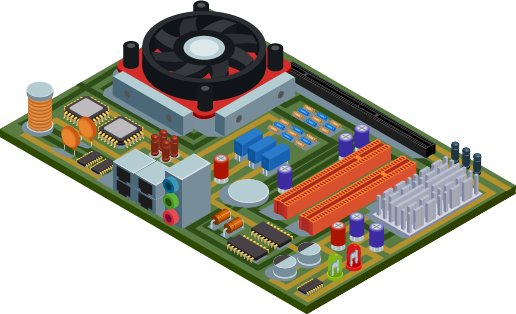
The rapidly evolving market today demands quick product development cycles. This fast pace presents a challenge, particularly for PCBA design teams where qualified workers are in short supply and are hard or impossible to replace.
Recognizing this, many teams now use design reuse strategy as an efficient countermeasure. By reapplying successful circuitry and designs, these lean teams can streamline their design process. Rather than starting from scratch and building new designs, they adapt and enhance existing layouts. This accelerates product development and rollout.
Ultimately, design reuse empowers PCBA design teams to achieve more with fewer resources, providing an agile workflow that can swiftly respond to dynamic market needs.
Benefits of Design Reuse
Applying existing designs throughout the entire design process can lead to significant savings in time and resources. Many PCBA layouts and designs use similar circuitry for power supplies, drivers, memory, etc, allowing developers to leverage these for basic functionality and save valuable design and troubleshooting time. It is advantageous to use established designs since they have already been tested in real-life applications.
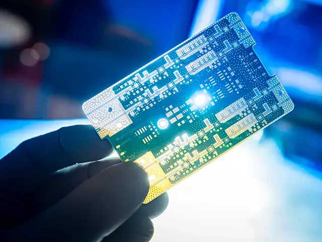
Signal integrity analysis and simulation are time-consuming aspects of the development process, especially when high-speed memory interfaces are involved that can lead to signal crosstalk and/or reflections, which can degrade signal integrity. These kinds of unpredictable potential issues have already been vetted into existing, established circuitry.
When the time comes to deliver a product to the client, existing designs with compatible connectors that have already been successfully integrated into a customer’s system save troubleshooting time for the customer as well.
Taking the idea a step further, PCBA developers can design basic templates for modular PCBA layouts with common components that designers can use as a foundation for more intricate designs with enhanced functionality. For instance, a designer could swap out the interface board on a PCBA board template for another wireless interface without having to swap out the processor or the storage boards as well.
Developers will still have to adjust their designs based on factors like form factor and physical board space, but it’s usually easier to tweak an existing design than to start from scratch. As a result, prototyping is usually faster and smoother.
In the aggregate, design reuse can result in shorter and more frequent development cycles, a wider range of products, and the opportunity to get those products to the market more quickly.
Ways to Effectively Implement Design Reuse
For an organization to fully realize the potential of design reuse, it usually requires the creation of a resource library that cross-references designs based on factors such as layout, components, and form factor.
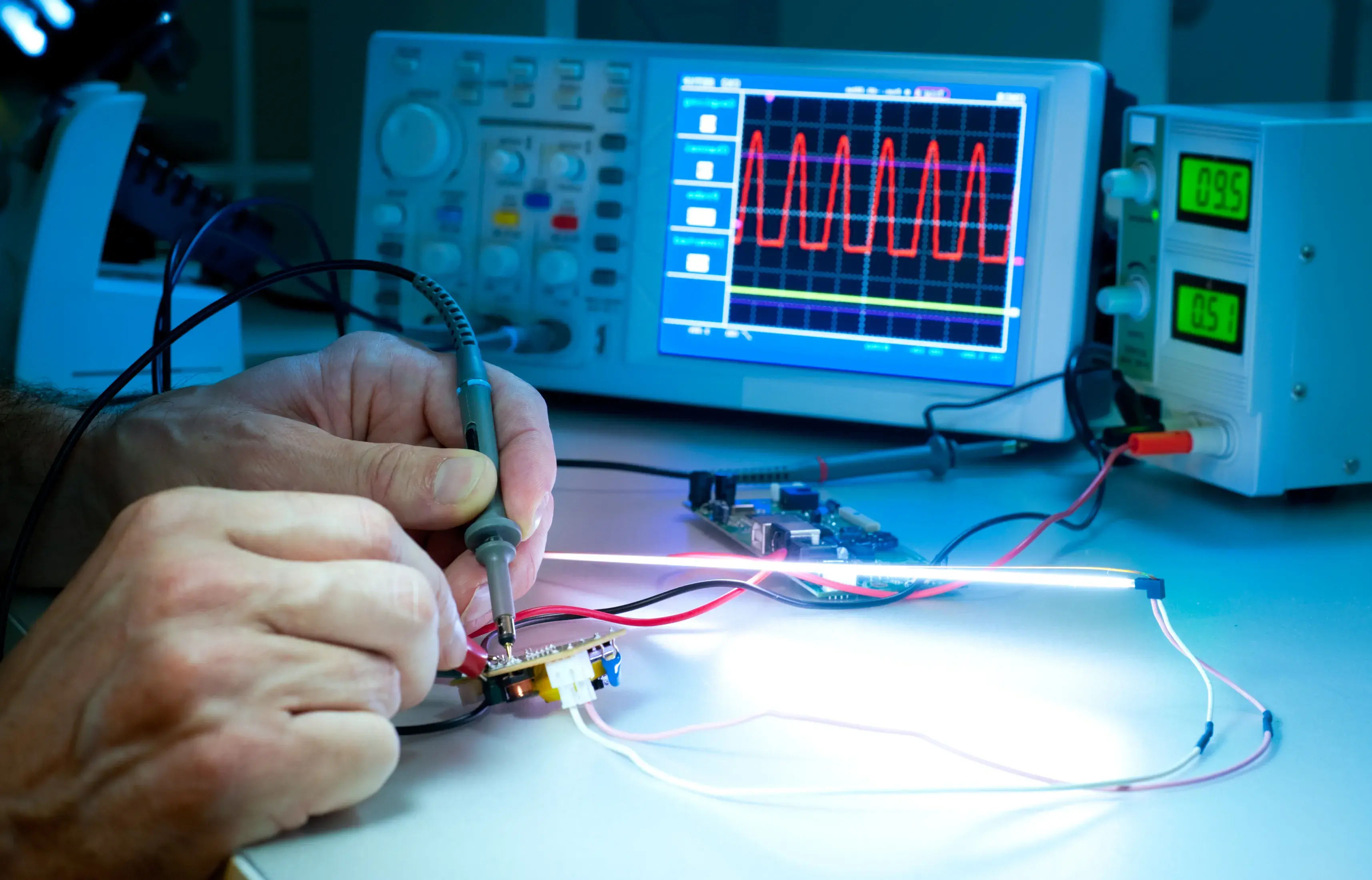
For example, a developer working on a project can look back on previous product designs for a specific customer to identify previously integrated components or connectors. Basic designs with commonly implemented components (i.e., power supply, processor, memory boards, etc.) can then be repurposed and modified to meet a different client’s needs without having to start from scratch.
By thinking of PCBA design as moving chess pieces on, off, or around the board, modular design practices make this kind of cutting and pasting approach more feasible. Making an older design a viable solution for a new project could be as simple as swapping out a connector or an interface board. Modular design can also help in the development of product lines, like boards with the same basic layouts but with different processors or added functionality for different implementations.
Organizational awareness and communication is the prevailing factor, ensuring developers have access to one another’s schematics, templates, and PCBA layouts and the practical history of those designs, i.e. how they’ve performed in certain settings and implementations.
This shared knowledge can help avoid common design problems like connector wear after repeated insertions or power trace aging at high currents, information that can be extremely valuable in avoiding similar design issues in the future.
Initially, these advantages might not seem significant on a project-by-project basis, but over time, this kind of design sharing will have a cumulative effect on the bottom line.
The Future of Design Reuse in PCBA Design
While repeatedly reusing the same modules and components can enhance efficiency, it also risks design complacency. This occurs when developers prioritize tried-and-true solutions over innovative, creative ones.
It’s an issue PCBA developers should be aware of. However, the potential long-term benefits of design reuse are too crucial to overlook. Not only does this strategy alleviate developers’ workload, but it also simplifies the customer experience and trims down troubleshooting and beta testing time. Thus, for PCBA developers seeking to optimize their processes, embracing design reuse can be an obvious and sensible choice.
Related Topics
How to Shorten PCBA Production Lead Times with MacroFab
In the rapidly evolving electronics sector, extended production lead times are no longer tolerable, and minimizing these lead times is crucial for success.
From Garage to Growth: How Startups Scale with MacroFab
Scale your hardware startup smarter with MacroFab—prototype to production, U.S. manufacturing, instant quoting, and expert support every step.
PCBA Order Lead Time Report: Guidance for Lunar New Year 2025
With Lunar New Year coming up, MacroFab wants to ensure they give the best guidance when planning orders to continue meeting delivery guidelines.
Want more design tips? Download MacroFab’s
Engineering Essentials: The PCBA Design HandbookAbout MacroFab
MacroFab offers comprehensive manufacturing solutions, from your smallest prototyping orders to your largest production needs. Our factory network locations are strategically located across North America, ensuring that we have the flexibility to provide capacity when and where you need it most.
Experience the future of EMS manufacturing with our state-of-the-art technology platform and cutting-edge digital supply chain solutions. At MacroFab, we ensure that your electronics are produced faster, more efficiently, and with fewer logistic problems than ever before.
Take advantage of AI-enabled sourcing opportunities and employ expert teams who are connected through a user-friendly technology platform. Discover how streamlined electronics manufacturing can benefit your business by contacting us today.