Via in pad is the design practice of placing a via in the copper landing pad of a component. Compared to standard PCB via routing, via in pad allows a design to use smaller component pitch sizes and further reduce the PCBs overall size. With component manufactures pushing smaller parts every year and the demand from consumers for smaller devices, the usage of via in pad practices by hardware engineers have become more commonplace. In this article, we will discuss the differences between via in pad and traditional vias, when should you use via in pad, and how to design for it.
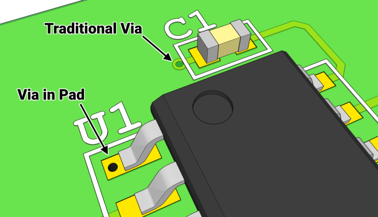
What Makes Via-in-Pad Different From Traditional Vias?
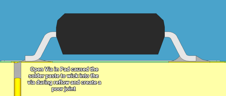
With traditional vias, the signal is routed away from the pad and then to the via. This allows the application of soldermask to prevent solder paste from wicking into the via during the reflow process. In doing so, this prevents a situation which can cause the pad and component connection to fail due to insufficient solder. With via in pad, the drill hole for the via is inside the pad. This means you can not tent the via with soldermask. Leaving the via open to allow the paste to wick into the barrel will cause reliability problems during manufacturing.
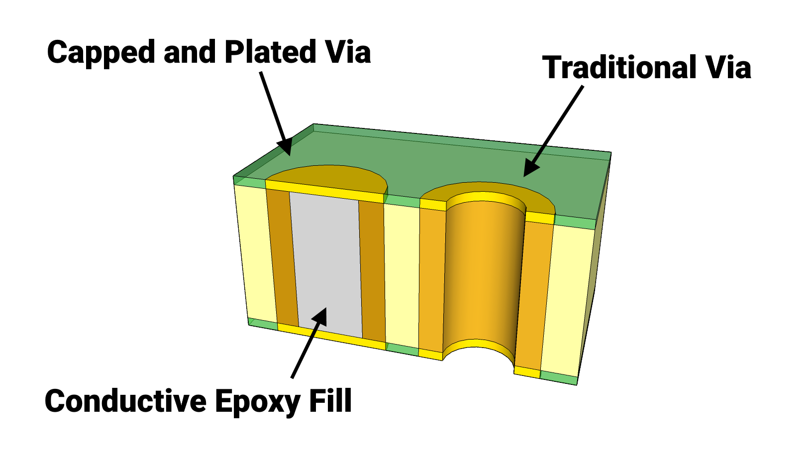
To reduce manufacturing defects and increase yield, it is best to implement via in pad by having your PCB manufacturer cap the via. This is accomplished by first filling the via with a conductive epoxy and then plating over with copper. Most contract PCB assembly manufacturers will not allow via in pad without first filling and then plating over the via.
When Should I Use Via in Pad?
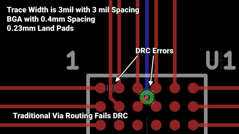
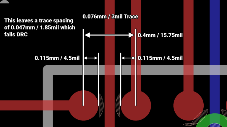
Trying to route and escape component packages with sub 0.5mm pitch with traditional routing methods will cause Design Rule Check errors due to trace width, annular ring, and drill size limitations. Manufacturing limitations on trace size does not allow for smaller and more compact traces to be made with traditional PCB fabrication methods. For these small pitch components, the only effective way to route them is with capped via in pad as this allows the PCB routing to be as compact as possible.
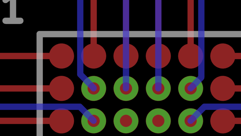
Capped via in pad can simplify routing for complex BGA and LGA packages as well. Instead of the traditional fan out, the signals can go straight into the PCB. Surface routing is minimized which can allow components like bypass capacitors to be placed as close as possible to other components, minimizing parasitic inductance. Also, this enables shorter paths to power and ground planes which will help minimize EMF emissions of high-frequency designs.
Vias in thermal pads can also help with heat management. High power surface mount parts typically have a thermal pad that mounts to the PCB. To dissipate the heat more efficiently, it is wise to drop vias through the PCB to the other side of the PCB to increase the copper area for heat release.
Why not use via in pad for every via then? The advantage gained in reducing component fan out and routing complexity is offset by increased manufacturing complexity and material costs of the PCB fabrication process. If the hardware design can be accomplished with traditional style via routing then it is best to avoid via in pad.
Designing for Via in Pad
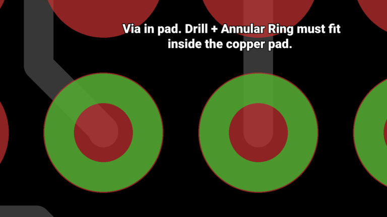
Implementing via in pad is very similar to traditional vias. What differs is how it affects the design rule checks for the PCB and how the manufacturing files are created. You will need to make sure your via in pad meets the manufacturer’s minimal annular ring requirement. The pad size of the component’s footprint must be equal to or larger than the minimal annular ring size. This is usually not an issue as most pad sizes are larger than vias but as BGA packages get smaller this will become a design problem to overcome. If the landing pad’s diameter for the BGA is smaller than the combined via and annular ring diameter, then using Solder Mask Defined pads will be your best bet. Consult the part manufacture for more information.
To properly manufacture PCBs that have via in pads, an additional manufacturing file is necessary. Besides the standard excellon drill file that is required, a drill file that just contains the vias that are in component pads and need to be capped and filled is also needed. Using two separate files reduces confusion on which vias need to be capped and reduces manufacturing cost by making sure traditional vias do not get filled and capped. Consult your EDA tool to see if there is an option to do this. If not, modifying your drill file with a Gerber viewer might be needed to create this extra file.
Exceptions to Always Capping Via in Pads
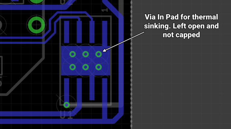
With most design rules there are exceptions and the “Always cap via in pads” is no exception to that rule! Center pads on QFN packages and thermal center pads for surface mount power parts generally benefit to having open via in pads. Without vias in the center pad of a QFN you can sometimes get trapped gasses or a lifting motion during reflow. These can cause the component to tilt to one side and lose coplanarity to the PCB. The vias in the center pad allow gasses made from the flux in the solder paste to more easily escape and also allows any excess solder paste that is under the part to be drawn through. With thermal pads this extra solder paste that fills the vias has the benefit of improving the thermal conductivity of the via.
Conclusion
With electronic components ever shrinking smaller, hardware engineers will need to utilize and learn new tools and techniques to implement these components in a reliable and scalable way. Via in pad allows the smallest component fan out possible with current PCB construction techniques. When looking at using via in pad techniques, consider the extra manufacturing cost and time that places on your product’s bill of materials. Make sure to work closely with your contract PCBA manufacturer as they will be able to give suggestions in regards to how via in pad can change the manufacturing process. Most manufacturers will agree that if your hardware design can be implemented without via in pad, then for cost and reliability reasons the design should avoid via in pad.
Ready to get started?