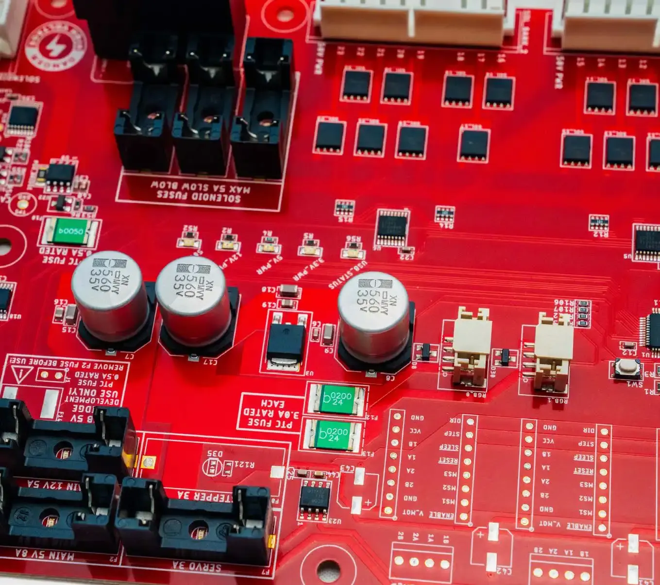
Unleashing Creativity: AI-Powered Exploration in PCB Design
Electronic design thrives on innovation, but keeping pace can be a challenge. Electrical engineers are constantly pressured to develop groundbreaking products quickly. Traditionally, translating these ideas into ˚physical layouts has relied heavily on the assistance of PCB designers. While this collaboration is vital, it can be time-consuming.
This is where Artificial Intelligence (AI) steps in. AI-powered PCB design assistants are shaking things up by offering a powerful tool: the freedom to explore.
Identifying Alternate Design Avenues, Fast
Imagine an experienced electrical engineer tasked with creating a prototype for a novel smart device with various sensors. Traditionally, such a complex layout utilizing multiple components in a restricted space would involve collaborating with a PCB designer to create a single layout.
Checkpoint
AI design tools offer engineers a key benefit: freedom from limitations.
However, with AI design tools, the engineer can explore many possibilities. These tools can generate several variations of the same PCBA, each with different dimensions, connector placements, and design constraints.
This ability to rapidly explore diverse options is a game-changer. It empowers engineers to experiment with various design concepts before settling on a final layout. This translates into several advantages:
- Sharper Design Choices: Visualizing multiple layouts allows engineers to make more informed decisions about size, performance, and manufacturability.
- Faster Time to Market: Exploring design options upfront can significantly reduce the time needed to finalize a layout, accelerating product development cycles.
- Enhanced Innovation: AI design tools liberate engineers from the constraints of traditional methods, allowing them to explore more creative and innovative solutions.
Beyond Exploration: Freedom from Constraints
AI design tools offer engineers a key benefit: freedom from limitations. Traditionally, requesting modifications from a PCB designer can be a time-consuming process. While collaboration is crucial, AI design tools offer additional flexibility.

This newfound freedom empowers engineers to be more creative and efficient in their design process. Take a company like Quilter, for instance. Their software utilizes reinforcement learning to generate multiple PCB layout options that meet an engineer's specifications. This allows engineers to experiment with different design iterations and explore a wider range of possibilities, ultimately leading to a more innovative final product.
Engineers can then focus on their core strengths – innovation and exploration. Quilter's software facilitates a more iterative design flow, enabling engineers to explore various configurations and arrive at an optimal solution faster. As a result of this streamlined workflow, PCB designers get pre-tested configurations from which to build the final design, thereby saving time for both parties.
Parker and Stephen talk to Sergiy Nestorenko of Quilter on this classic Circuit Break episode, about his journey from SpaceX to transforming PCB design with artificial intelligence.
The Power of Machine Learning
At the core of these AI design tools lies a powerful technology called machine learning (ML). Machine learning algorithms are essential computer programs that can learn from data, and they typically learn in one of two ways: supervised learning from existing layouts, or from reinforcement learning using simulation within a controlled environment.
In simulation learning, ML algorithms are trained on massive datasets of past successful PCB designs. These datasets include existing board layouts, design rules, and performance parameters. By analyzing these examples, the AI learns the relationships between component placement, routing strategies, and desired outcomes like signal integrity and thermal management.
In reinforcement learning (the kind Quilter uses), the AI acts like a grad student in a virtual PCB design lab. It gets to experiment with countless layouts, but its grade depends on following real-world rules. These rules consider things like physics (think keeping electromagnetic interference under control) and how easy it would be to build the board using standard practices while keeping costs down. By rewarding layouts that excel in these areas and penalizing designs with issues, the AI can explore new possibilities and potentially discover innovative solutions that traditional methods might miss. This process of experimentation and feedback allows the AI to continually improve its design capabilities.
Those of you who were raised on 1980s movies may recall the last scene in WarGames where Joshua (certainly an AI) takes over NORAD's systems and begins playing every possible variant of thermonuclear war until he realizes there is no winning move. This kind of repeated simulation and analysis is similar to the kind of reinforcement learning many AI tools use today.
The Future of PCB Design with Faster Manufacturing
The potential of AI-powered design tools is clear. By offering engineers the freedom to explore and experiment, these tools can significantly improve the efficiency and creativity of the PCB design process.

Further, AI can act as a bridge between design and manufacturing. By incorporating knowledge of different manufacturers' supported stack-ups and design rule sets, AI tools can propose layouts that are inherently manufacturable with CM services like MacroFab. This eliminates the need for rework later in the process, streamlining the transition from design to fabrication and accelerating the entire journey from idea to finished product.
As AI technology matures and machine learning algorithms become even more sophisticated, we can expect more advanced tools that will further streamline the design workflow and empower engineers to bring their ideas to life in a much shorter timeframe.
Once you've finalized the perfect design with the help of AI exploration tools, services like MacroFab can handle your PCB assembly with incredible speed and precision. Their online platform allows for instant quotes, real-time DFM checks, and a streamlined ordering process, ensuring a smooth transition from design to high-quality production. The combination of AI design and MacroFab allows your innovative ideas to reach the market faster than ever before.
Related Topics
The Impact of AI on PCBA Design: What You Need to Know
Providing a balanced perspective on how AI can revolutionize PCBA design while also looking at the challenges that we can face with this new technology.
How EMS Manufacturing Benefits from Human-AI Teamwork
The benefits of AI are clear faster decision-making, better integration, and increased efficiency, to name a few.
Ready to Get Started?
Get an instant quote nowAbout MacroFab
MacroFab offers comprehensive manufacturing solutions, from your smallest prototyping orders to your largest production needs. Our factory network locations are strategically located across North America, ensuring that we have the flexibility to provide capacity when and where you need it most.
Experience the future of EMS manufacturing with our state-of-the-art technology platform and cutting-edge digital supply chain solutions. At MacroFab, we ensure that your electronics are produced faster, more efficiently, and with fewer logistic problems than ever before.
Take advantage of AI-enabled sourcing opportunities and employ expert teams who are connected through a user-friendly technology platform. Discover how streamlined electronics manufacturing can benefit your business by contacting us today.