Turning your brilliant ideas into a tangible product is an exciting process. This journey requires navigating several crucial steps, and one of the most critical is translating your concept into a physical Printed Circuit Board (PCB). The PCB is the foundation, holding and connecting all the electronic components that bring your design to life.
While the schematic serves as the blueprint for your circuit, outlining a netlist of how the components connect to each other, manufacturers primarily rely on Gerber files and drill files for PCB fabrication. Gerber files define the physical layout of each layer in the PCB, including copper traces, solder mask, and silkscreen. Drill files specify the location and size of holes needed for through-hole component leads and via connections between layers.
Understanding schematics remains important as it provides a clear view of the circuit’s functionality. Some manufacturers, like MacroFab, will use a design’s schematics to check component rotation, ensure the PCB Gerber files were created correctly with a netlist, and debug any problems that may happen during production.
This comprehensive guide equips you with the knowledge to confidently navigate the early design phase, focusing on the importance of the schematic in conjunction with Gerber and drill files throughout the PCB creation process.
What is a PCB Schematic?
A schematic functions similarly to a detailed city roadmap and is a visual representation of your circuit’s electrical connections. This roadmap displays each component – resistors, capacitors, transistors, and integrated circuits (ICs) – using standardized symbols that are universally understood by electronics professionals. Lines (also called nets) connecting these symbols represent the conductive pathways, providing a clear illustration of how current will flow through your circuit.
| Component | Designator | Component | Designator |
|---|---|---|---|
| Battery | BT | Jumper | J |
| Capacitor | C | Metal Oxide Varistor | MOV |
| Crystal | X/Y | Oscillator | X |
| Diode/LED | D | Power Supply | PS |
| Fuse | F | Relay | K/EM |
| Heatsink | H | Resistor | R |
| Integrated Circuit | U/IC | Switch | SW |
| Zener Diode | D or Z |
PCB Schematic Standards
Two main standards govern schematic notation around the world:
IEC 60617 (Graphical Symbols for Electrical and Electronic Diagrams)
This international standard, published by the International Electrotechnical Commission (IEC), provides a comprehensive collection of graphical symbols for various electrical and electronic components. It covers many components used in circuit diagrams, including resistors, capacitors, transistors, integrated circuits, switches, relays, connectors, and more.
Impact on PCB Schematics:
-
IEC 60617 ensures consistency in schematic symbols used across different countries and design teams. This allows anyone reviewing a schematic, regardless of their location or background, to understand the circuit’s functionality based on the standardized symbols.
-
The standard promotes clear and unambiguous representation of components, minimizing the risk of misinterpretations during PCB design and manufacturing.
ANSI/Y32.2 (Graphic Symbols for Electrical and Electronic Diagrams - American National Standard)
This standard, developed by the American National Standards Institute (ANSI), is the US counterpart to IEC 60617. It provides a collection of graphical symbols for electrical and electronic components, with a focus on symbols commonly used in North America.
Impact on PCB Schematics:
-
ANSI/Y32.2 offers a familiar reference point for engineers and designers in the US who are accustomed to these symbols.
-
While largely aligned with IEC 60617, there might be slight variations in some symbol representations between the two standards. This is important to consider when collaborating with international teams or encountering schematics created outside the US.
The Relationship Between IEC 60617 and ANSI/Y32.2:
While these are separate standards, there’s a significant overlap between them. In many cases, the symbols defined in IEC 60617 are directly adopted by ANSI/Y32.2. This promotes international understanding and consistency in schematics. However, some minor differences might exist for specific symbols or components.
Overall, both IEC 60617 and ANSI/Y32 play a critical role in ensuring standardized and unambiguous representation of components in PCB schematics. This promotes clear communication between designers, manufacturers, and anyone involved in the development process, leading to the creation of reliable and functional electronic devices.
The Power of a Precise Schematic in PCB Design
An accurate and well-defined circuit board schematic lays the groundwork for your entire design process. A meticulously crafted PCB schematic translates into a functional, efficient, and reliable PCB. Providing the netlist, a detailed definition of how various components like resistors and capacitors are connected, creates a rulebook in text format for how connections will work.
Clarity and precision are paramount when creating a schematic. Using clear and consistent symbols ensures anyone reviewing your design, from your colleagues to contract manufacturers, can grasp its functionality quickly.
Why is Your PCB Schematic Important?
The PCB schematic remains a vital part of the PCB creation process, even though Gerber files and drill files are used for manufacturing. It acts as the foundation for your design, much like a blueprint for a building.
Here’s why your schematic is important:
-
Clear Communication: The schematic acts as a universal language, visually depicting components and their connections. This clarity is crucial for both internal teams and external manufacturers. While Gerber files provide manufacturing instructions, the schematic offers a deeper understanding of the circuit’s functionality, promoting smoother collaboration and troubleshooting.
-
Fewer Errors: By visualizing connections beforehand, the schematic helps identify potential errors early in the design phase. This reduces the risk of mistakes that could lead to costly rework or malfunctioning PCBs.
-
Foundation for Manufacturing: While not directly used in production, the schematic informs the creation of the layout of the PCB Assembly which then creates the Gerber files and drill files. It specifies component types and their interactions, ensuring the manufacturer has a clear picture of the circuit’s design intent.
-
Documentation & Maintenance: A well-documented schematic becomes an invaluable reference throughout a PCB’s lifecycle. It allows for easier maintenance, modifications, and future troubleshooting by anyone familiar with standard schematic symbols, even if they aren’t familiar with the specific Gerber file used for manufacturing.
How to Craft a Clear and Functional PCB Schematic
Creating a PCB schematic – the blueprint of your circuit – requires adhering to specific standards for clarity and functionality. Let’s delve into the key aspects of effective schematic design:
Standardized Page Setup:
-
Page Size: Most design tools offer various page sizes. Choose one that accommodates your circuit complexity.
-
Page Naming: Divide complex schematics into logical blocks on separate pages named alphabetically. This simplifies navigation for reviewers.
Grid System (Optional):
While not mandatory, a grid system within your design software can provide valuable reference points. It helps with component placement, connection clarity, and network probing during inspection.Page Title Block:
Include essential details in the schematic footer, such as page size, revision number, date, and circuit name/function.Adding Comments:
Explanatory notes enhance understanding. You can incorporate comments directly on the schematic or on separate pages for complex designs. Annotations might cover jumper states or PCB layout constraints.Revision History:
Track design changes with a revision history log. This document details the date, description of modifications, reviewer and author names, and review comments. Typically, it resides on the final schematic page. Most people use version control software like github or the like to handle revision and commit history.Large Projects: Schematic Directory (Optional):
For intricate designs, a directory listing all topics within the schematic documentation aids in locating specific modules. Skip this step for smaller, simpler projects.Block Diagrams (Optional):
For complex circuits, block diagrams visualize different modules and signal flow, significantly improving design comprehension during review.Layered Schematics (For Complex Designs):
When your PCB stack-up comprises numerous modules, consider employing a layered schematic structure. This hierarchy clearly shows the signal flow between modules. Clicking on a module reveals its detailed view.Component Reference Designators:
Standardized reference designators identify components in a schematic. These follow IEEE guidelines and use uppercase letters.Component Symbols:
Utilize pre-existing symbols from the design software's library whenever possible. Common components include resistors, capacitors, transistors, and integrated circuits (ICs). For uncommon components, consult the manufacturer's datasheet for symbol creation guidance.Heterogeneous Components:
Components with numerous pins, such as microprocessors, often require special attention. To maintain clarity, represent different sections of a single package as distinct components within the schematic.Network Connections:
Whenever two wires cross and share an electrical connection, depict this junction with a clear interface element within the schematic.Network Labels:
Network labels enhance schematic readability. Instead of drawing numerous connections from an IC, refer to a designated net name associated with a specific pin on another device. Pins with the same name are assumed to be connected. Network labeling isn't necessary when connecting directly to another IC on the same page.Component Placement:
Strategic component placement within the schematic impacts the bill of materials (BOM) and IC package creation later in the design process.Design Rule Checking (DRC):
Utilize the DRC feature within your design software to identify potential errors based on predefined design rules. This helps ensure the schematic's logical and physical integrity.Netlist Verification:
Upon completing the schematic design and initiating the layout process, generate a netlist file. This file (.mnl or .txt) details all electrical connections between components. Manually verify the netlist to prevent design errors.Bill of Materials (BOM):
Most design software offers BOM generation functionality. If you provide all necessary component details during symbol creation or library import, the software can generate a comprehensive and accurate BOM. BOM information typically includes the manufacturer part number (MPN), package type, supplier name, and supplier part number.Schematic Checklist (Optional):
Consider creating a schematic checklist to minimize errors and enhance overall design quality. Remember, a well-crafted schematic is the foundation for a successful PCB layout and ultimately, a functioning electronic device.Want to know more about schematics and connectors? Listen to this classic Circuit Break podcast episode now.
Essential Symbols You’ll Encounter: Understanding Diagram Language
While minor variations might exist between regions, circuit board schematics rely on a specialized visual language made of symbols that generally adhere to common standards established by the IEC and ANSI. You can decipher how circuits work if you understand these symbols.
Symbols You'll See on a Schematic:
- Resistors: These are depicted in two standardized forms. Consistent use across the schematic is vital. The unit for resistance is the ohm (Ω). Remember to maintain consistent unit usage throughout the design. Input all relevant component details into your design software.
- Capacitors (Polarized and Non-Polarized): Unlike their non-polarized counterparts, capacitors have positive and negative terminals. Incorrect polarity can lead to damage. The IEEE standard defines the capacitor symbol. Ensure the pin code assigned to the symbol accurately reflects the physical component’s pinout.
- Transistors and Mosfets: These workhorse components have three terminals: base, collector, and emitter. When mapping pin layouts to schematic symbols, always reference the component’s datasheet. When creating symbols, include a depiction of the actual component for future reference, especially when replacing obsolete parts.
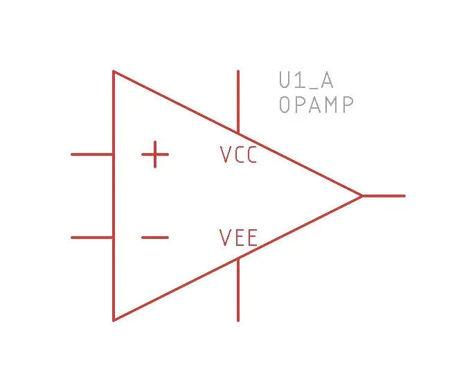
- Operational Amplifiers (Op-Amps): Create op-amp symbols following IEEE standards. While some designers prioritize convenience, strive for clarity. Place all input pins on one side and all output pins on the opposite side. Similarly, position power and ground pins at the top and bottom, respectively. Be cautious when flipping or rotating symbols, as positive and negative terminals might swap positions.
- Heterogeneous Components: Complex devices like FPGAs, memory, and microprocessors have numerous pins for various functions (data lines, address lines, control lines, power supply). For improved readability, break down these components into multiple symbols within the schematic.
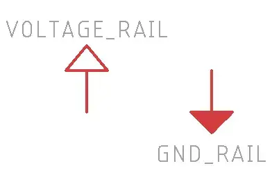
- Power and Ground Symbols: Standard symbols represent power supply and grounding pins. Since negative voltages might exist on the board, use ”+” to indicate voltage. Establish a consistent and reliable method for representing voltage levels and their connections within the circuit.
Listen to this classic episode of the Circuit Break Podcast to learn about measuring op-amp input impedance.
Ensuring Schematic Accuracy: A Checklist for Inspection
Verifying all elements within the schematic is crucial during PCB design, considering Design for Manufacturability (DFM) principles. Here’s a checklist to streamline the process:
- Verify Component Details: Cross-check component pin assignments and labels against the datasheet for accuracy.
- Polarity Matters: Double-check polarity for all polarized components.
- No Overlaps: Ensure no label overlaps with pins for clarity.
- Transistor Check: Confirm that the transistor base, collector, and emitter pins match the datasheet.
- Component Review: Verify component value, reference designator, and placement.
- Complete Notation: Ensure all schematic elements have proper notation (MPN, supplier name, part number).
- Off-Page Connections: Check for off-page connectors to ensure proper connectivity.
- Inter-Table References: Identify any inter-table references within the schematic.
- Decoupling Capacitance: Verify decoupling capacitance for all integrated circuits. Separate ground pins based on signal type (analog, digital, signal, ground).
- BOM Accuracy: Review the Bill of Materials (BOM) for quantity and part number accuracy.
By understanding these core concepts and following this inspection checklist, you’ll be well-equipped to navigate the world of circuit board schematics with confidence.
PCB Design Software: A Schematics’ Best Friend
While creating a schematic by hand is certainly possible, good PCB design software saves time and simplifies the process significantly. These software tools offer a comprehensive suite of features to transform your schematic into a production-ready PCB layout.
Here are some of the valuable functionalities PCB design software provides:
-
Schematic Capture: This core function allows you to create and edit the schematic diagram of your PCB using a user-friendly interface. Drag-and-drop functionality for components and intuitive net labeling tools expedite the process.
-
Symbol Libraries: Software packages come pre-loaded with extensive libraries containing standardized symbols for a vast array of electronic components. This ensures consistency and clarity in your schematics.
-
Component Datasheet Integration: Many circuit board design software tools allow seamless integration with component datasheets. This enables you to access critical information about each component, such as its specifications, pinouts, and recommended footprints, directly within the design software.
-
Connectivity Verification: These software tools perform automated checks to ensure all connections within your schematic are valid and consistent. This helps identify errors like missing connections or unintended shorts early in the design phase.
-
PCB Layout Tools: PCB design software goes beyond schematic capture. It offers a powerful set of tools for translating your schematic into a physical PCB layout. These tools include features for placing components, routing traces, and defining the PCB stackup.
-
Design for Manufacturability (DFM) Checks: Advanced software incorporates DFM checks that analyze your PCB layout for potential manufacturing issues. These checks identify areas where the design might be difficult or impossible to fabricate, allowing you to rectify them before sending your files to the manufacturer.
Choosing the Right PCB Design Software: A Balancing Act
The PCB design software landscape offers a wide range of options, each catering to different needs and experience levels. Here are some key factors to consider when making your choice:
-
Complexity of your Design: For simple circuits with few components, free or open-source software might be sufficient. However, for intricate designs with high-speed signals or dense component placement, feature-rich professional software might be necessary.
-
Ease of Use: If you’re new to PCB design, prioritize software with an intuitive interface, comprehensive tutorials, and a supportive user community.
-
Cost: Software options range from free and open-source to premium, subscription-based models. Evaluate your needs and budget to make the best choice. Some software offers limited free versions with basic functionalities, allowing you to test-drive the software before committing to a paid plan.
Understanding and Reading Circuit Board Schematics
Circuit board schematics offer a wealth of information on how a circuit functions, similar to a construction plan or course syllabus. Grasping how to read these schematics is essential for anyone venturing into the world of electronics.
Essential Elements:
-
Component Designations: Each component in a schematic has a unique identifier called a reference designator (REFDES). This code combines a letter signifying the component type (R for resistors, C for capacitors) with a number (R3, C1) for easy identification.
-
Visual Language: Schematics use standardized symbols to represent actual components soldered onto the PCB. These symbols ensure universal understanding of the circuit’s function.
-
Network Connections: Networks, depicted as lines connecting component pins, represent electrical connections within the circuit. Following these network paths reveals signal flow.
Key Outputs:
- Netlists: After schematic design, PCB layout software generates netlists. These comprehensive lists of electrical connections guide designers in placing and wiring components on the actual PCB.
- Bill of Materials (BOM): A BOM is a detailed list of all components used in the schematic, including their corresponding physical components and part numbers. The BOM format varies based on schematic complexity and component database.
By understanding these core elements, you’ll be well-equipped to navigate the intricacies of circuit board schematics.
Partnering with a Reliable PCB Manufacturer: From Design to Prototype
Once your PCB layout design is finalized, it’s time to translate your design into a tangible product. Here at MacroFab, we offer a user-friendly online platform that simplifies the PCB manufacturing process. Upload your design files, specify your requirements (material selection, number of layers, etc.), and receive high-quality PCBs delivered straight to your doorstep.
Our advanced manufacturing capabilities cater to a wide range of complexities, from simple single-layer PCBs to intricate multilayer designs. We also offer a variety of material options to suit your specific needs, such as high-frequency laminates for RF applications.
Read more about turning your schematic into a tangible product now.
Beyond Fabrication: Additional Services to Streamline Your Development
MacroFab goes beyond simple PCB manufacturing. We offer a comprehensive suite of additional services to streamline your development process, including:
-
Assembly: Our team of experienced professionals can handle the assembly of your PCBs, including component placement, soldering, and functional testing.
-
Enclosure Design and Box Build: We offer services to design and prototype custom enclosures to house your PCBs, creating a complete and functional product.
-
Design for Manufacturability (DFM) Review: Our team can review your design files and provide expert feedback to ensure your PCBs are manufacturable and meet industry standards.
Conclusion: Bridging the Schematic to PCB Gap with Confidence
The path from schematic to PCB might seem complex at first glance, but with the right knowledge, tools, and partners, it can be an empowering and rewarding journey. By understanding the core concepts of schematics and PCB design, leveraging powerful PCB design software, and partnering with a reliable manufacturer like MacroFab, you can bridge the gap between your concept and a functioning electronic prototype.
This comprehensive guide equips you with the foundational knowledge to navigate the schematic-to-PCB workflow. MacroFab stands ready to support you throughout your entire development process, from design review to high-quality PCB manufacturing and assembly.
Upload your schematic to MacroFab today and experience the seamless transition from concept to prototype!