When designing footprints for diodes it is important to place clear indicating marks to show the components orientation. Since diodes are polarized components (they have to be placed in a certain orientation) they must have indicating marks on the PCB to help determine how they should be placed. Clarity in marking components is key to making sure that the manufacturing of your design goes smoothly.
Let’s take a look at good methods of marking diodes.
The Diode
Here is the schematic symbol for a diode:

Diode Schematic Symbol
The two terminals for a diode are marked cathode and anode. When creating a footprint for a diode we must indicate which terminal connects to which pad. All diodes will have a physical marking on the body of the component indicating how placement should occur on the footprint. In most cases, the mark on the physical case of the diode will represent the cathode of the device but it is important to note that this is not always true!
Here is an example of a datasheet for a 1N4148 diode showing the component and how it is marked:
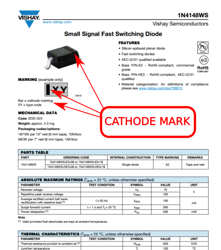
1N4148 Diode Datasheet
For this component, the physical marking on the device represents the cathode pin of the diode.
Designing The Footprint
When we design footprint files for the diode, we should have a way to clearly indicate this pin placement. A good footprint should be easy to understand and read. Since diodes are normally marked on the package where the cathode is located we should place some information on the footprint to indicate this. Here is an example footprint of a diode:
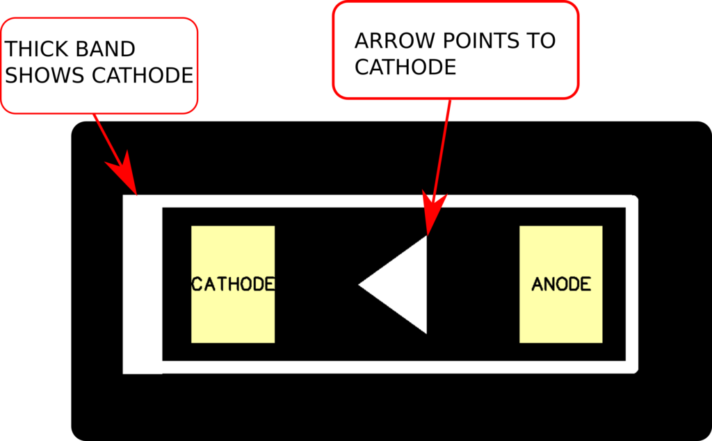
Cathode Marked Diode Footprint
In this footprint there are two forms of indication. First the silkscreen near the cathode pad is thicker and second, there is an arrow in between the pads that points to the cathode similar to how the schematic symbol of a diode looks. Having two forms of indication may at first seem overkill, but when you consider that the diode will be placed on top of the arrow indicator it makes sense to have the second indicator external to the component’s placement.
Footprint Files: Breaking the Rules
Even though diodes are typically marked on the package where the cathode pin is located, there are exceptions to this rule. Diodes can occasionally have makings on the package indicating the anode pin. Because of this it is very important to carefully review the datasheet of every diode/LED that you plan to use in your design.
Here is an example of two red LEDs from the same manufacturer. Both LEDs are red and come in a 0805 sized package. Looking carefully at the part markings, one has a package indicator pointing to the cathode and the other to the anode.

Datasheet Comparison
Making footprints for anode marked components is similar to cathode marked components with the exception of the silkscreen maker. For anode marked components, the silkscreen marker should indicate the anode.
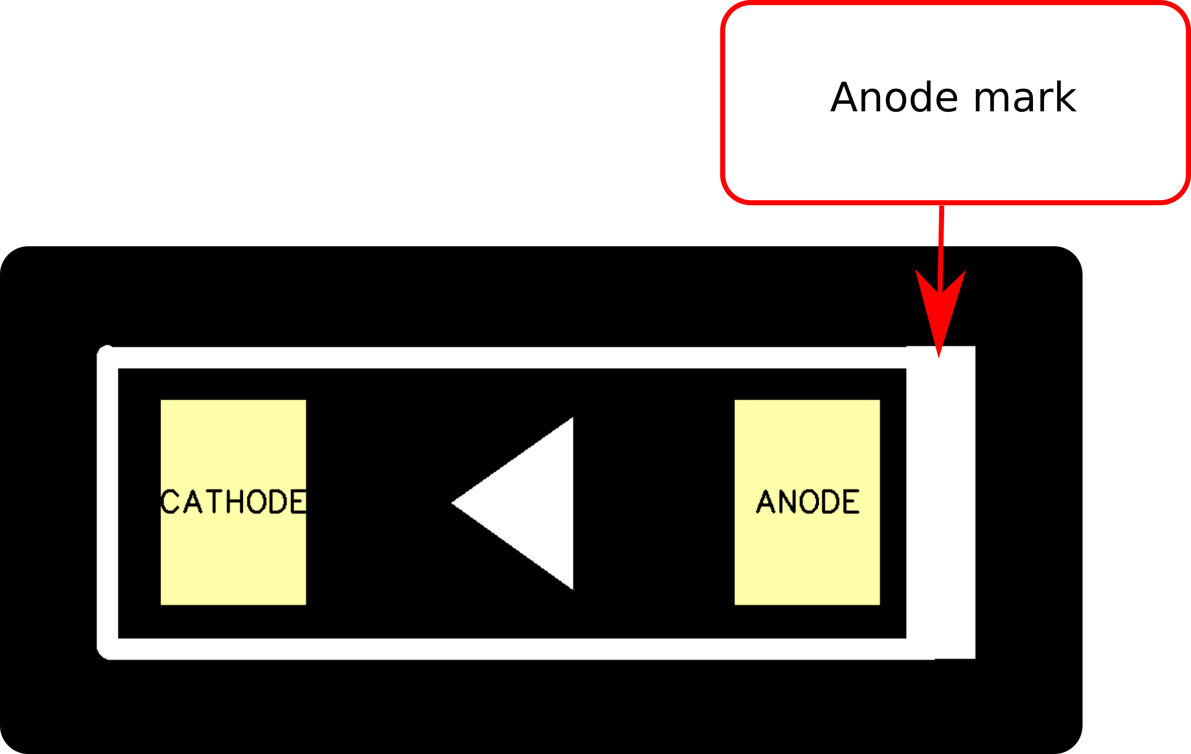
Anode Marked Diode Footprint
Odd Form Diodes
For diodes that come in odd shaped packages or for those that have more than two pins the same rules of marking the footprint to match the package apply. Lets take a look at the MacroFab RGB led part number MF-LED-3228-RGB. This part has three LEDs in one package with 4 leads arranged in a common anode configuration. The package had a notch indicating where pin 1, the common anode is located. Placing a clear indicating mark on the footprint to represent this pin 1 notch is key. The following image shows the datasheet drawing for the part and the footprint side-by-side. The footprint has a large dot near pin 1 indicating that the part should be placed with the notch facing this pad.
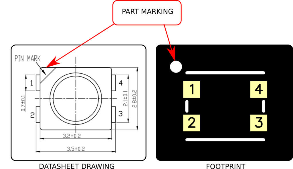
MacroFab MF-LED-3228-RGB footprint
The next post in this series is called: The Footprint Files – Electrolytic Capacitors
Was this post helpful? Are there other topics you’d like us to discuss? If so, let us know on Twitter.