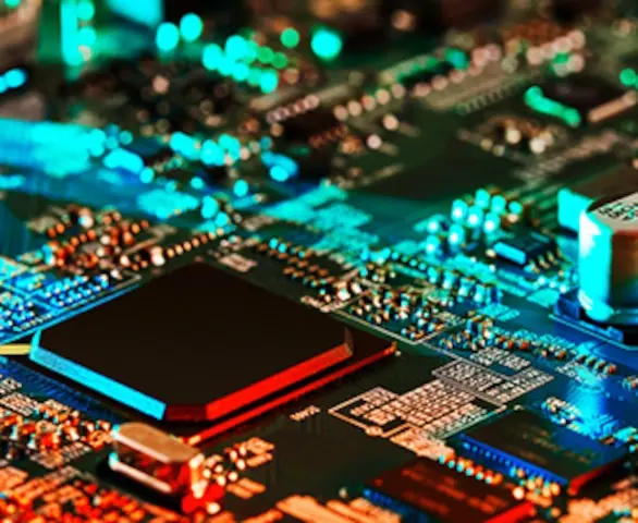
Protect PCBA Designs From Reverse Engineering: Tips and Tricks

Imagine pouring countless hours, resources, and brainpower into designing the perfect Printed Circuit Board Assembly (PCBA) for your cutting-edge product. It’s a labor of love, a technical masterpiece. Then imagine someone else, a competitor perhaps, quickly reverse engineering your design, essentially decoding your hard work and using it to their advantage. That’s a scenario no innovator–or innovative company–wants to face.
Reverse engineering (RE) is a real and persistent threat in the world of electronics. It is performed to glean a product’s inner workings, replicate, create similar or better products, or, in worst-case scenarios, infiltrate a system to exploit vulnerabilities. Undeniably, it’s a threat that can potentially undercut your market position and dilute your product’s unique value proposition.
However, guarding against RE, or ‘hardening’ your PCB assembly design, can drive up development time and manufacturing difficulty, creating a more expensive bill of materials (BOM).
This article offers valuable tips and effective strategies on how to protect your PCBA designs from various reverse engineering techniques so that it’s more challenging, time-consuming, and expensive for anyone to reverse engineer them, from both hardware and software perspectives.
Understanding Piracy of Intellectual Property (IP) in Hardware
IP refers to creations of the mind, such as inventions, literary and artistic works, designs, symbols, names, and images used in commerce. In the hardware world, IP can manifest as proprietary technologies or a reusable unit of logic, cell or unique design layouts, and custom software algorithms, among other things.
Hardware IP piracy involves the unauthorized use or duplication of another’s hardware design or proprietary technology. This can take several forms in the PCBA industry:
- Unauthorized Replication: This is a common form of IP piracy where an entity copies a PCBA design without permission. They may manufacture identical or near-identical units, often sold at a lower price. It hurts the profits of the original developers through unfair competition and can harm their brand reputation if counterfeit products are of inferior quality but are confused with the originals.
- Technology Theft: This involves the theft of proprietary technology developed by a company. A competitor might reverse engineer a product to gain access to its technical secrets and then use those secrets to create their own products. This kind of piracy can dilute a company’s competitive advantage.
- Trademark and Brand Piracy: This form of piracy involves the unauthorized use of a company’s branding or trademarks. For instance, a pirate may manufacture PCBAs that are visually identical to a legitimate product, complete with counterfeit logos and branding. This can mislead consumers and damage the reputation of the original brand.
IP embodies the heart and soul of your product – it is the unique blueprint that distinguishes your work from others. Defend your hardware IP from adversaries who are capable of reverse engineering, piracy, and malicious changes.
Understanding the Purpose of Reverse Engineering
Reverse engineering, often seen as the art of ‘undesigning,’ involves disassembling an existing product to understand its inner workings, designs, and structures. Like solving a complex puzzle, the final image is known, but finding how the pieces fit together is the challenge.
The goal of reverse engineering PCBAs is manifold. On one hand, it is useful for benign applications like analyzing the PCBA for potential enhancements, identifying and fixing faults (chip- and board-level failure analysis and testing), ensuring compatibility with other products, or re-creating a previous design that has lost its documentation. It is benign, however, only if the original IP owner consents and knows about it.
In contrast, a malicious party could reverse engineer your PCBA to extract your intellectual property. They could then use your IP for the creation of products for sale or integration into their own products without compensating you, the rightful IP owner. Besides reverse engineering, they might also find security vulnerabilities in your IP, exploit them later, or even add a backdoor once they gain a white-box understanding of it.
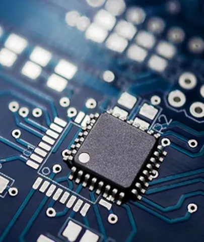
Techniques Used in Reverse Engineering of PCBAs
PCBAs consist of PCBs, which are constructed with layers of thin copper foil (conductive) layers laminated to insulating (non-conductive) layers. These layers form the physical foundation for electronic components and provide electrical pathways between them. By disassembling the PCBA and imaging each individual copper layer of the PCB, it is possible to reverse engineer the entire PCBA layout.
Key techniques used in reverse engineering a PCBA include:
- Solder Mask Removal: The solder mask is a protective layer covering most of the PCBA, preventing solder bridges from forming between closely spaced pads. However, it also hides the copper traces beneath. The primary goal of this process is to expose the copper traces on the top and/or bottom layers with minimal damage.
- Delayering: This is a destructive technique used to access the inner copper layers of a multi-layer PCB. The aim is to reveal the circuitry on each layer of the PCB, which is particularly useful when dealing with complex, multi-layer designs. Like solder mask removal, this technique is typically used on unpopulated PCBs. Dremel tools, CNC milling machines, and surface grinders can be used for delayering.
- Imaging: The technique can be used even on fully populated PCBs as it helps document the PCB’s design and layout at different stages of reverse engineering. This process involves the use of X-ray inspection equipment, which allows for internal imaging without physical disassembly or delayering
Why Protect Your PCBA Designs from Reverse Engineering?
Your PCBA designs are more than just circuit layouts and component lists; they’re the embodiments of your unique ideas, countless hours of development, and substantial investment in research and development (R&D).
Checkpoint
Not securing your PCBA designs can lead to financial losses due to reduced market share and eroded profit margins, but it can also affect customer and partner trust.

The implications of not securing your PCBA designs from reverse engineering are significant. Not only can it lead to financial losses due to reduced market share and eroded profit margins, but it can also result in a loss of trust from your customers and partners. If your product can be easily copied and sold at a lower price, why should customers remain loyal to your brand? Furthermore, it could discourage your R&D team, who may feel their hard work and innovation are not adequately protected.
But the threats aren’t just from competitors. If your PCBA designs contain security-sensitive elements or is used as part of a security-sensitive device, reverse engineering can lead to vulnerabilities being exploited, causing severe harm to your customers and potential legal repercussions for your company. A 2020 article in IEEE Spectrum noted that “the vulnerabilities of the printed circuit board itself are only now starting to get the attention they deserve.”
Moving into an increasingly global economy, IP protection cannot solely rely on passive methods such as patents and copyrights. While these provide legal recourse, the enforcement of such rights can be a complex and expensive process, especially when infringements occur in jurisdictions with different legal systems and attitudes toward IP protection.
Therefore, a more active form of protection is necessary – one that makes reverse engineering your PCBA designs a more difficult, time-consuming, and costly endeavor. This is where obfuscation techniques come into play.
Want to know more about how we keep your designs safe? Read Securing Data in Electronics Manufacturing: MacroFab’s Approach now.
Strategies for Obfuscating PCBA Designs
Obfuscation refers to the practice of deliberately making a product more difficult to understand or decipher by hiding its true meaning or functionality to protect the IP inherent in the product.
Here are some key strategies for obfuscating your PCBA designs during the design process:
Sealing the PCBA or parts of the PCBA in epoxy:
This technique involves encapsulating the entire PCBA or specific critical components in a layer of epoxy resin. Epoxy sealing provides a physical barrier that makes it difficult to access or tamper with the PCBA, thereby hindering reverse engineering attempts.
However, sealing the PCBA in epoxy may make repairs and maintenance more challenging. Additionally, the epoxy itself can add weight and bulk to the final product. Moreover, epoxy can change the thermal properties of your board and lead to other design challenges.
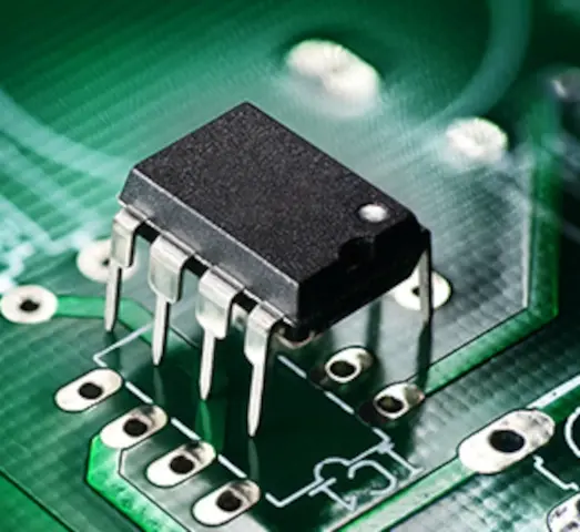
Washing the markings off ICs:

This method entails removing the identifying markings from the integrated circuits (ICs) on your PCBA, making it more difficult for someone to determine which components are being used.
Washing off IC markings can impede reverse engineering efforts by making it harder to identify the specific components and their functions within the design. In some cases, designers go so far as to rename components with misleading identifiers that will confuse potential hackers. But, a skilled reverse engineer might still be able to identify the ICs based on their physical characteristics.
Using blind vias:
Blind vias are non-through holes that connect one external layer of a PCB to one or more internal layers but do not pass through the entire board. By using blind vias in your PCBA design, you can make the circuit layout more challenging to decipher, as connections between layers become less obvious.
Nonetheless, blind vias can increase manufacturing complexity and costs, as well as reduce the overall reliability of the PCBA due to potential issues with the interconnections between layers.
Using a custom IC:
A custom IC, also known as an application-specific integrated circuit (ASIC), is designed specifically for your product and tailored to perform a unique function. An ASIC makes it more difficult for competitors to reverse engineer your design, as they would need to design their own IC or find an off-the-shelf alternative that may not offer the same performance or functionality.
However, custom ICs can be expensive to develop and manufacture, particularly for smaller production runs. Additionally, you may face challenges related to sourcing and supply chain management, as you’ll be dependent on the specific IC provider for continued availability. In addition, you should consider how you will keep all documentation relating to the ASIC secure for the foreseeable future.
Other Protection Techniques to Consider
Further security may be provided by tamper detection or encryption on any programmable device on your PCBA. Regularly updating and patching software or firmware can also help to protect any programmable component against reverse engineering.
Protecting hardware from copying often involves programming an MCU in One-Time-Programmable (OTP) mode, disabling external data access. This includes turning off JTAG and debug facilities. However, this strategy restricts debugging and remote updates, limiting improvements to system integrity or service quality.
Certain MCUs, like Texas Instruments’ MSP430FR family, offer secure methods for on-chip memory access. It allows either password-based JTAG port security or complete disablement. It also enables the creation of secure and non-secure zones within the memory space using IP Encapsulation (IPE), with the secure area impervious to external access but permitting intra-area data interaction.
Other MCUs, like the Microchip PIC32MZ family, have a built-in hardware crypto engine. This engine supports common encryption and decryption ciphers, like AES, DES, and Triple DES, and uses a secret key for data protection. It also provides hardware-implemented data authentication. This hardware crypto engine’s performance is vital for systems requiring frequent, high-volume data processing, like during high-speed transmissions or boot processes.
Read why some industries are leveraging design reuse as part of their product development plan.
Threats in the Supply Chain
While much of the focus on PCBA protection is geared towards external threats such as reverse engineering by competitors, it’s crucial not to overlook potential threats within your supply chain. Supply chain threats can occur at your design house or at the PCBA manufacturer.
Design House:
This is where the ideation and creation of your PCBA design occur. Threats at this stage can come in various forms:
Sometimes, the risk comes from within. Disgruntled employees, for example, could leak sensitive design information. Unsecure networks or insufficient cybersecurity measures can also leave your designs vulnerable to hacking or unauthorized access.
PCBA Manufacturing Partners:
The production stage also presents its own set of challenges:
Unscrupulous manufacturers: When outsourcing manufacturing, particularly to overseas partners, there’s a risk of IP theft if your designs are not adequately protected. Unscrupulous manufacturers might sell your designs to other parties or use them to produce unauthorized versions of your product.
Unauthorized Production: Some manufacturers might be tempted to produce more units of your product than agreed upon. These unauthorized units could be sold without your knowledge, cutting into your profits and potentially damaging your brand’s reputation. To mitigate these risks, there are non-engineering tactics you can use.
Non-engineering Methods for Protecting PCBA IP Design
Beyond technical obfuscation and embedded security measures, several non-engineering methods can further secure your PCBA design IP. These strategies involve the careful selection of partners and the strategic management of your designs.
- Pick a Trustworthy Manufacturer: Choose your manufacturing partner carefully. An ethical, trustworthy manufacturer is a cornerstone of protecting your PCBA designs. Conduct due diligence, check references, and establish solid contractual agreements that bind the manufacturer to respect and protect your IP.
- Manufacture Under Robust IP Laws: Opt for countries with robust IP laws, such as the United States or Mexico. These countries have well- established legal frameworks that safeguard intellectual property and provide recourse in case of infringement.
- Maintain Digital Design Control: Retain digital control of your design at all times. Limit access to your design files and securely store them using encryption or other cybersecurity measures. This ensures that only authorized personnel can access and modify your design data, reducing the risk of unauthorized use or leakage.
- Contracts and Non-Disclosure Agreements (NDAs): Legal agreements play a crucial role in IP protection. A well-drafted contract or NDA can provide substantial legal protection for your designs, offering a clear recourse in the event of a breach.
Remember, while engineering methods are crucial for protecting your PCBA designs, these non-engineering strategies offer valuable additional layers of security. They may not be the first line of defense, but they are certainly an important part of a comprehensive IP protection plan.
Conclusion
The threat of reverse engineering is real, and the consequences, ranging from lost profits to brand reputation damage, can be severe.
As we’ve explored, various methods can help secure your designs – from obfuscation techniques to embedding “Easter eggs” in code and addressing supply chain threats. Each approach has its pros and cons, and the most effective strategy is often a combination of these methods, tailored to your specific needs.
By implementing a multi-faceted approach, you’ll be well-equipped to safeguard your valuable PCBA designs from reverse engineering threats and maintain your competitive edge.
Related Topics
Struggling with Inflexible PCB Assembly? MacroFab's Got Your Back.
Many electronics designers struggle with systems that demand complete data and specific formats upfront. Wouldn't it be great if there was a better way?
Fab Insights: HASL vs ENIG
Choosing the right surface finish for a PCBA can be tricky. HASL and ENIG differ in their methods of coating printed circuit boards.
How Do QFN Packages Compare to Other Surface Mount ICs?
This article aims to arm electrical engineers and PCBA designers with comprehensive insights into the QFN package.
Read more about PCBA Design Essentials
Download MacroFab’s Engineering Essentials: The PCBA Design Handbook
About MacroFab
MacroFab offers comprehensive manufacturing solutions, from your smallest prototyping orders to your largest production needs. Our factory network locations are strategically located across North America, ensuring that we have the flexibility to provide capacity when and where you need it most.
Experience the future of EMS manufacturing with our state-of-the-art technology platform and cutting-edge digital supply chain solutions. At MacroFab, we ensure that your electronics are produced faster, more efficiently, and with fewer logistic problems than ever before.
Take advantage of AI-enabled sourcing opportunities and employ expert teams who are connected through a user-friendly technology platform. Discover how streamlined electronics manufacturing can benefit your business by contacting us today.