Prototyping for product development demands creativity, knowledge sharing, and staying current with advancing technology. Yet, tight deadlines often push engineers to take shortcuts, potentially costing time and resources in later stages of development. Here are some guidelines to help you be proactive during this process.
The Right Time to Transition: From Breadboard to Custom PCB
A skilled engineer can quickly generate concepts and prototypes using breadboards and off-the-shelf components to prove feasibility. Development boards, breadboards, and basic wiring are often enough to test simple concepts.
However, there are limitations to what can be accomplished with off-the-shelf parts and the transition to a custom PCB becomes necessary.
In some cases, using off-the-shelf boards can prove out a concept and a team can go confidently into development, including designing a custom PCB. These typically include simple low voltage, digital circuits.
However, off-the-shelf solutions are limited, especially for more complex projects. In these cases, transitioning to a custom PCB is essential. Situations where a custom PCB is required include:
- **RF-Based Applications: **PCB trace impedances and parallel capacitances must be precisely analyzed.
- **Complex Circuits: ** Multiple sensors, peripherals, or voltage rails, and high-power applications requiring thermal management.
- **Prototypes for Ergonomic Testing: **Custom-shaped PCBs are often necessary to test the final product’s form factor with users.
Moving to a custom PCB at the right stage ensures accurate testing, better iteration, and a smoother transition to production.
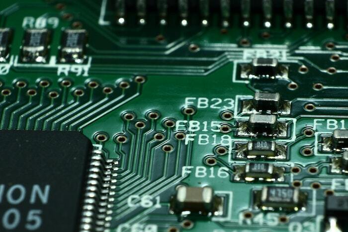
Avoiding Common Pitfalls in PCB Design
Tips for Schematic Capture and Layout
When ready to move into schematic capture and layout, be cautious of the decisions made. These decisions have a high probability of making their way into production even if doing so was not the intention.
Deadlines, resource constraints, and budget limitations will commonly be the reason why specific aspects of a product will be deemed acceptable and not revised.
When changes need to be made after a product has transitioned to the manufacturing design phase, board level changes can become problematic. Changing the schematic or layout may require testing to be redone which can waterfall into having to rewrite test protocols and obtain re-approvals.
This could easily add weeks to the development timeline. Having a component become obsolete early in the production phase can lead to a shortage of stock on the shelf, limiting profits for the company. In addition to development hurdles, changing the PCB design later than anticipated can cause designs to fall out of compliance. Use a pre-order checklist for prototypes before moving on to manufacturing to make sure you’re ready for this step.
Prototyping for NPI: Strategies for Timely Development
New Product Introduction (NPI) relies heavily on efficient prototyping. Avoiding common shortcuts can improve timelines and project success. Here are key practices to keep in mind:
Reusing Legacy Designs: A Risky Proposition
You run the risk of obsolete parts in older designs, and those files may not utilize the latest technology in PCB manufacturing that could enable the design to be more space efficient. Additionally, other issues may arise such as net name inconsistencies and outdated footprints.
The Perils of Using Lab Scrap Components (op-amps, transformer cores, MOSFETs, etc.)
Components laying around in the lab should be avoided unless they have been properly stored and they are accurately labeled. IC’s can be faulty without showing any signs of damage leading to a week’s worth of debugging.
Navigating Niche Components: A Cautious Approach
Sometimes niche components cannot be avoided, but ensure your requirements are accurate and your design does not get cornered. For example, a 155ohm resistor may be exactly what is needed for a filter, but changing other components may allow for 150ohms and a multitude of backup options should the part go obsolete.
Read why component obsolescence begins at design now.
Building Strong Prototyping Habits: Keys to Long-Term Success
When designing a PCB assembly, anticipating where the prototype will be two iterations from now will pay off in the end and can save unneeded frustration. Not all product specifications and inputs may be readily available early in development. Design for a broad range of potential inputs.
If it is a battery-powered application, be prepared for the chance that it could require more power than originally anticipated. If 20W of power is needed for the initial concept, the next iteration may require 30W. Designing for and incorporating a higher-capacity battery may end up saving a design revision and a few weeks of turnaround time.
One of the best habits an engineer can develop is good PCBA documentation. A design will likely go through multiple iterations both formally and informally.
Early on in the process, document the circuit, its purpose, how it works, and its expected behavior. When the first boards arrive, they will go through component changes, cut traces, and air wiring until they function as intended. Unless each step is documented along the way, replicating those changes in the next revision will be difficult and prone to mistakes. (Note: when you use MacroFab’s technology platform, all your design iterations get automatically saved, so you can go back at any time to see how your design has changed over time.)
Another good habit that will save time is to always order extra prototype boards. Permanently damaging a board can come unexpectedly and at inopportune times. The benchtop supply was set too high or a component was shorted while being probed causing a pad to be burned are just a couple of examples. Having extra boards on hand will prevent having to wait to continue testing.
Working closely with supply chain and manufacturing teams from the beginning will also identify high-risk components and assembly challenges. Engaging a contract manufacturer (CM) with a robust supply chain network can streamline sourcing and secure alternatives for unavailable or end-of-life components.
It is important to remember that, more often than not, the first PCB for a new concept will likely not be the final one. Be prepared to make iterations, keep track of changes, and work cross-functionally early on to avoid delays during development.
Learn how cloud manufacturing can help you with your rapid prototyping needs.
When you’re ready to prototype your PCB, using a CM with online capabilities will help you keep your files better organized, rather than emailing different versions of your designs and keeping track in your inbox.
Embracing Connected Technology Manufacturing for Rapid Prototyping
Using a CM with online capabilities, such as MacroFab’s technology platform backed by FabIQ, enables better file management and reduces the need to juggle multiple versions across email. FabIQ leverages advanced AI to provide instant, accurate pricing for PCB assemblies, streamlining the transition from prototype to production. By analyzing your design files, FabIQ delivers competitive pricing tailored to your needs, whether you’re working on a single prototype or scaling up for mass production.
Additionally, FabIQ automatically identifies and recommends engineer-approved, form-fit-function component alternatives, addressing supply chain challenges and reducing time spent searching for parts. This intelligent platform not only accelerates the prototyping phase but also ensures a seamless progression into full-scale manufacturing, making your workflow more efficient and cost-effective.
Prototyping is just the first step in product development. By following best practices, engineers can ensure a smoother transition from prototype to production while maintaining focus on delivering high-quality, scalable designs.
Turnkey PCBA Prototyping
Rev up your design game, iterate faster, and build better products within one comprehensive technology platform.