Handling Silkscreen Over Component Pads
One of the issues commonly seen in PCB design is silkscreen information overlapping exposed copper on pads. If the ink from the silkscreening process is on a pad that is to be soldered it will likely inhibit the solder from flowing and will result in a bad joint. In general, it is a good idea to never have silkscreen on any exposed copper that is to have solder applied.
When the Gerber files are sent to a board manufacturer they are typically reviewed for issues including silkscreen on pad. In most cases, the manufacturer will adjust the Gerber information to prevent this by removing or moving the overlapping information. Although these issues are typically caught it is not good design practice to rely on it.
In some cases, the manufacturers will not make changes and create a board that has the issues (They make the board exactly as the Gerber files tell them).
Luckily, fixing silkscreen over component pads with EDA tools is simple. Getting into the habit of creating component footprints with no silkscreen over component pads is worthwhile and prevents issues in manufacturing.
The following picture shows a SOIC-8 package where the pad width was selected to be too long. The red boxes around show areas where the silkscreen (green in this example) overlaps the pads.
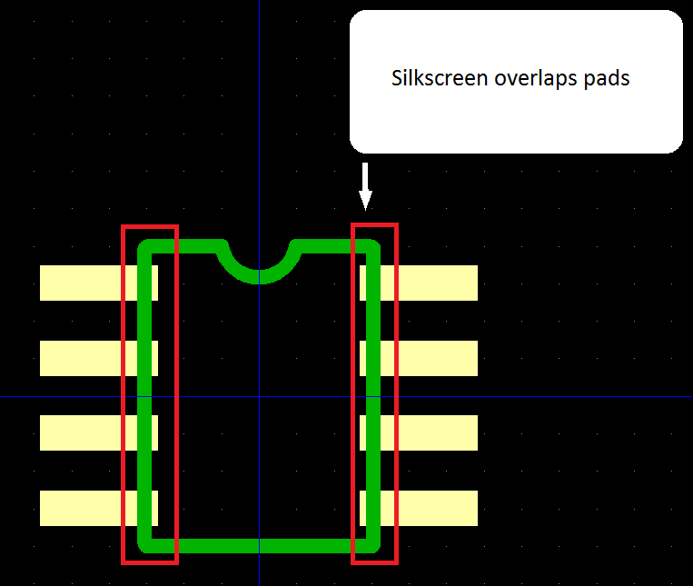
Image 1 1447177221379
The solution to this issue would be to reduce the width of the pads or move them further out from body of the component. In the following image the pads were moved from the body such that there is 0.01″ of space between the silkscreen and pad.
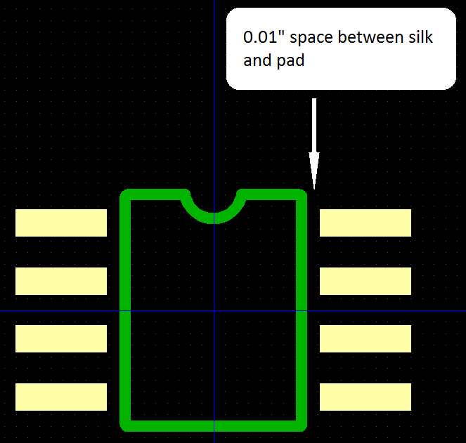
Image 2 1447177233459
0.01″ (10mils) is a good general number for spacing between silk and copper to prevent issues.
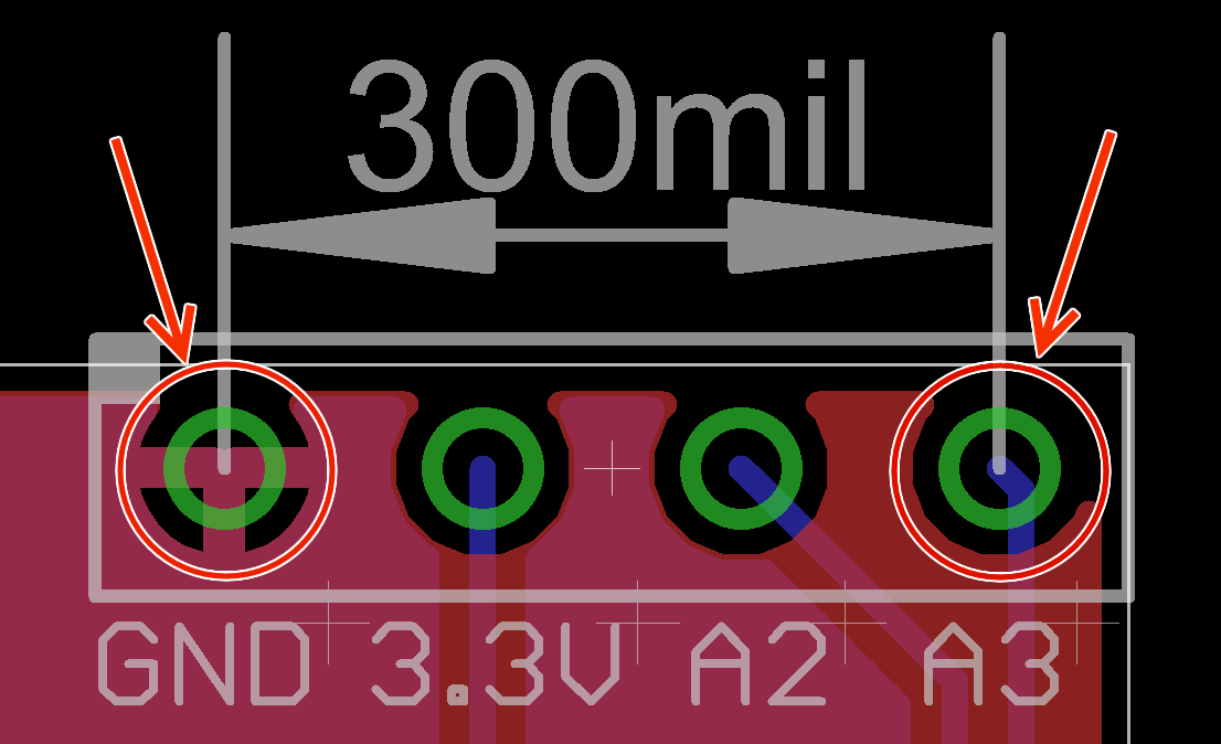
There are cases where the designer wants information such as dimensions and assembly information to appear on the board in their EDA tool. The following picture shows an example of dimension lines crossing into pads.
When adding such information, it is important to not use the silkscreen layer. In this case, the dimension layer 48 in Eagle was used to draw the dimension lines. The information on this layer is not included in the exported Gerber files that are sent to the PCB manufacturer and will not show up on the silkscreen.
Making sure that pads and exposed copper is free from silkscreen is good design practice and prevents manufacturing issues.
Related Topics
MacroFab vs. PCB Manufacturing Brokers: Why Direct Matters
This blog explores the key differences between MacroFab and manufacturing brokers, and why direct manufacturing is the optimal choice for PCBA needs.
Ultimate Guide To PCB Schematics: Concept to Prototype
A comprehensive guide for navigating early design phases and utilizing schematics alongside Gerber and drill files during the PCB creation process.
How MacroFab Uses Clear Communication to Improve Your PCB Production Experience
This blog will discuss how MacroFab can help customers in their PCB production experience through clear communication in a high-octane environment.
About MacroFab
MacroFab offers comprehensive manufacturing solutions, from your smallest prototyping orders to your largest production needs. Our factory network locations are strategically located across North America, ensuring that we have the flexibility to provide capacity when and where you need it most.
Experience the future of EMS manufacturing with our state-of-the-art technology platform and cutting-edge digital supply chain solutions. At MacroFab, we ensure that your electronics are produced faster, more efficiently, and with fewer logistic problems than ever before.
Take advantage of AI-enabled sourcing opportunities and employ expert teams who are connected through a user-friendly technology platform. Discover how streamlined electronics manufacturing can benefit your business by contacting us today.