PCB Cutouts, Slots, Routes, and Border Files: Revisited
MacroFab’s PCB Assembly supports plated and non-plated PCB cutouts, slots, and routes. The last time we touched on this subject was in the article Plated Slots: Stop Fitting Square Pegs in Round Holes where we explained why a PCB designer should use plated slots instead of large drills for connectors. In this article, I will show a couple examples of how to draw plated and non-plated cutouts and slots so we can build your PCB according to spec.
The Border Gerber File
MacroFab looks for cutouts and slots in the .BOR or border gerber file. In the EDA Tool Eagle this is generated from the Dimension layer 20. Other EDA Tools will call this the PCB border. If you are uploading an ODB++ package you will have to make sure the cut outs are drawn on with your border tool. You can check after uploading to MacroFab by reviewing the Border Layer in the PCB viewer. DRC rules for cut outs and slots can be found on our Assembly Specification Page.
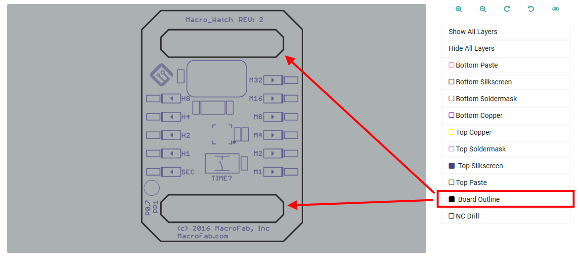
Macro Watch cutouts PC Bviewer
MacroWatch Example PCB. Checking if the cutouts exist in the PCB viewer.
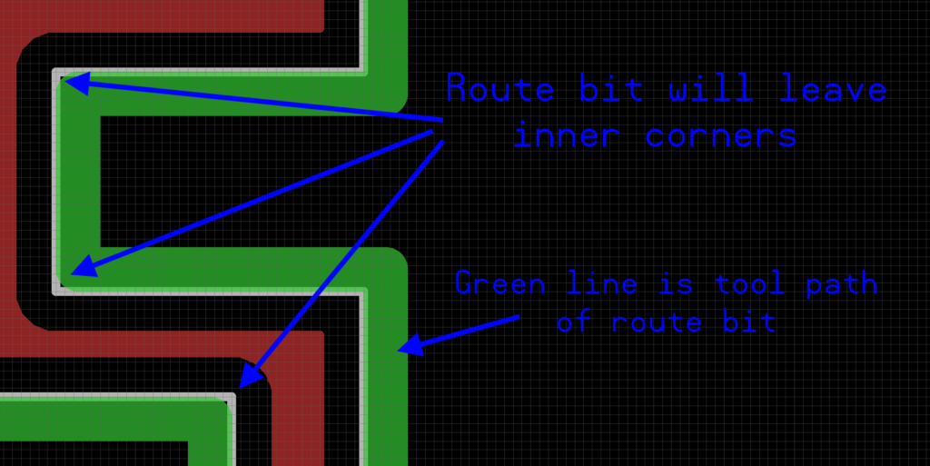
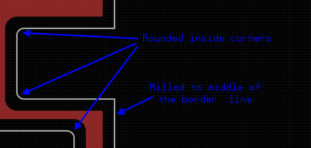
Make sure the width of the lines is at least 1 mil or larger. The board is milled/cut to the middle of the line, so thickness of the line does not impact the result. Making the thickness of the lines a non zero number will reduce problems down the road with external gerber viewers.
Drawing Cut Outs and Slots
I used Eagle as my example EDA Tool but others should follow suit to get the desired outcome. I drew the cut outs on the dimension layer for Eagle which is Layer 20. The red areas are Copper. The example shows three different kinds of cut outs or routes; external cut out, internal cut out, and internal plated cut out.
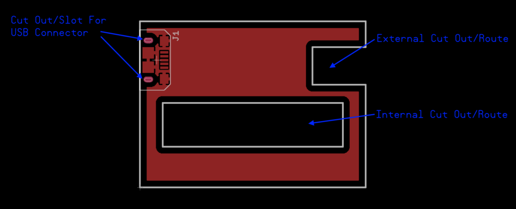
Example cutouts 1 1024x416
Example Board with three different types of cut outs or routes.
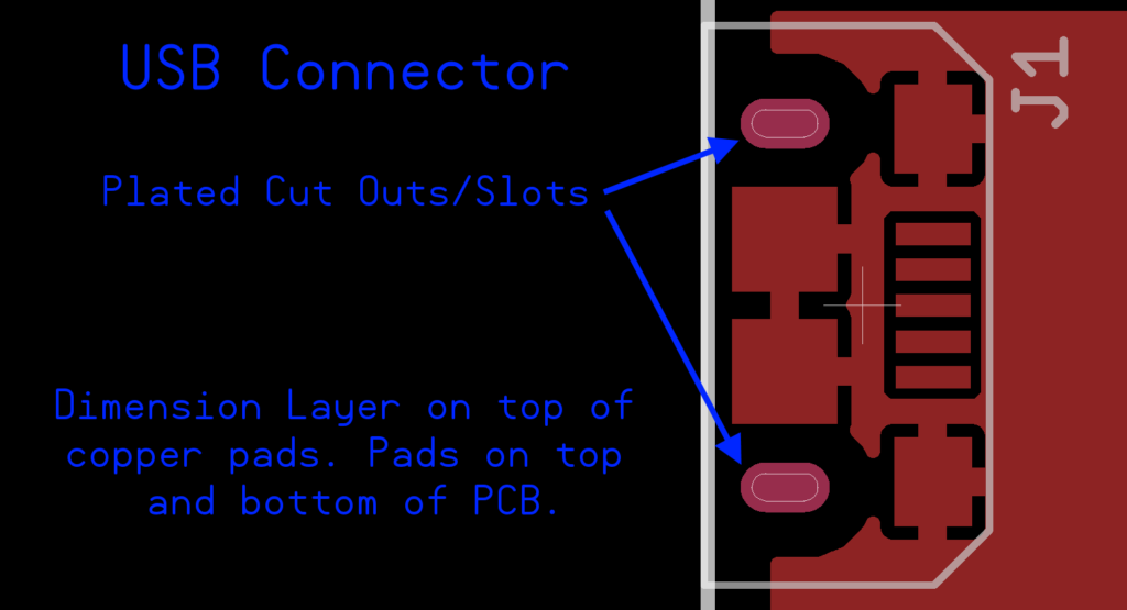
Example cutouts 2 1024x555
Close up of the USB connector which uses plated cut outs. The cut outs are drawn over the copper pads.
When uploaded to MacroFab, the cut outs can be seen in the PCB view under the Border Outline layer.
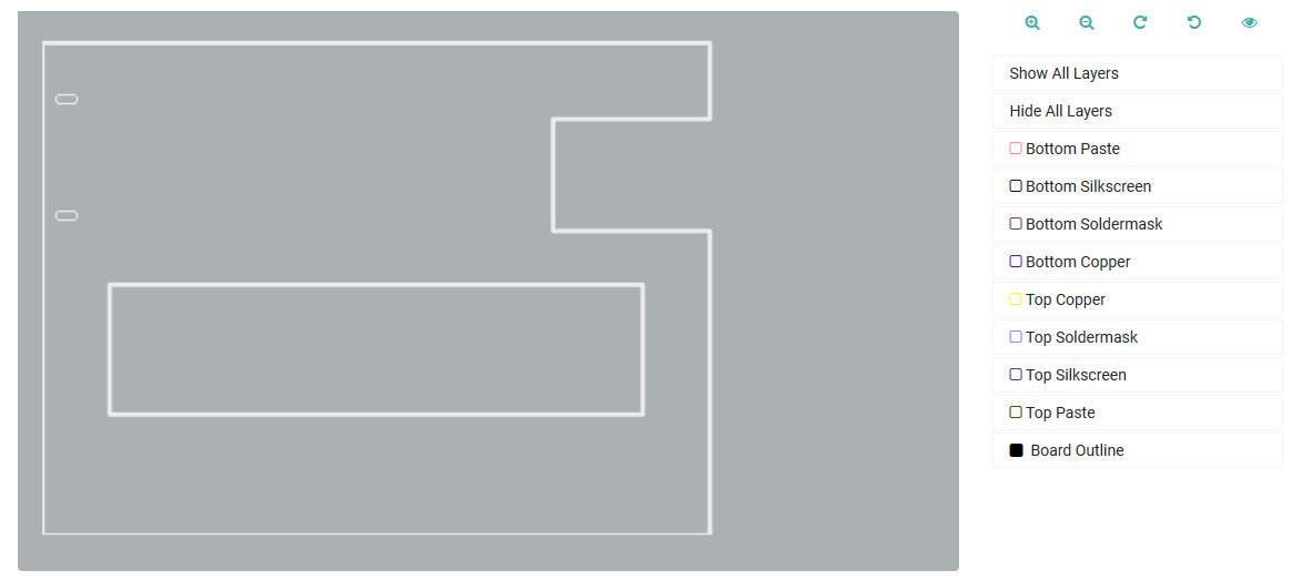
Example cutouts 3
MacroFab PCB viewer example cut outs
Non Plated or Plated Cut Outs?
If you draw your cut outs over copper it will be assumed to be a plated cut out. This is similar to a drill placed in the center of a copper pad for a via. For non plated, pull the copper back at least the recommended distance from copper to board edge DRC. That is all you need to do to denote the difference in your design files.
How the PCB will be milled
When the cut outs are machined out of the FR-4 material (what PCBs are made out of) the PCB fab uses a round bit similar to a CNC machine. Thus inside corners of cut outs will not be sharp but will have a round edge to them. This is something to watch out for in enclosure designs. The smallest inside corner radius possible at MacroFab is 0.5mm. This is because the smallest tool used for routing out boards is 1.0mm in diameter.
Example cutouts 4 1 1024x513
Below is what the above design will look like after the PCB is made. The inside corners are rounded and the edge of the PCB is cut to the middle of the border line.
Example cutouts 5 1024x490
What about external exposed plated cut outs?
Ah! Castellated Edges are an example of external plated cutouts. These are used on breakout boards and similar module style boards. We will be cover these in another article.
Recap
- Border gerber file should include all routes and cut outs
- Border lines will be cut to the middle
- Width does not matter
- Kerf of the bit will be in the waste area of the route or cut out
- Inside edges will be rounded due to router bit
- Route will be plated if through copper planes
Ready to get started?
About MacroFab
MacroFab offers comprehensive manufacturing solutions, from your smallest prototyping orders to your largest production needs. Our factory network locations are strategically located across North America, ensuring that we have the flexibility to provide capacity when and where you need it most.
Experience the future of EMS manufacturing with our state-of-the-art technology platform and cutting-edge digital supply chain solutions. At MacroFab, we ensure that your electronics are produced faster, more efficiently, and with fewer logistic problems than ever before.
Take advantage of AI-enabled sourcing opportunities and employ expert teams who are connected through a user-friendly technology platform. Discover how streamlined electronics manufacturing can benefit your business by contacting us today.