Circuit Board Testing Methods: What You Need to Know
Summary
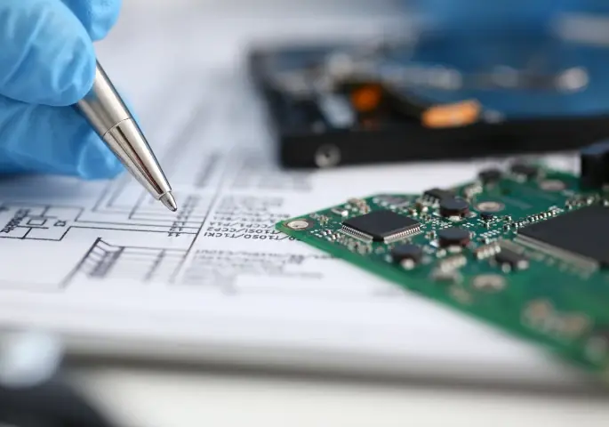
Circuit board testing is an essential part of the Printed Circuit Board Assembly (PCBA) manufacturing process. It helps identify and rectify potential issues before devices reach consumers, ensuring product integrity and customer satisfaction.
With so many electronic circuit board testing methods to choose from, it can be difficult to select the best one for your project. Here is a summary of the most common methods, along with their advantages, disadvantages, and best-suited applications:
Visual Inspection
- Visual inspection is the initial step in the testing process. It involves examining the PCBA for defects using the naked eye, magnification tools, or automated optical inspection (AOI) systems.
Advantages:
- Quick and cost-effective
- Can identify a range of defects, including misaligned components, solder bridging, and missing/damaged parts
Disadvantages:
- May overlook faults that aren't apparent to the naked eye, or those concealed beneath components
Best suited for:
- Identifying gross defects
- Screening for quality issues in high-volume production
High-quality electronics production relies on these testing methods to prevent malfunctions and ensure proper operation. However, with so many electronic circuit board testing techniques available, selecting the most suitable test procedure can be challenging.
To help make this decision easier, we provide a clear summary of the most common circuit board testing methods. By learning about these methods, you can improve your PCBA manufacturing process and ultimately elevate the quality of your electronic products.
Identifying Faults in Loaded PCBAs
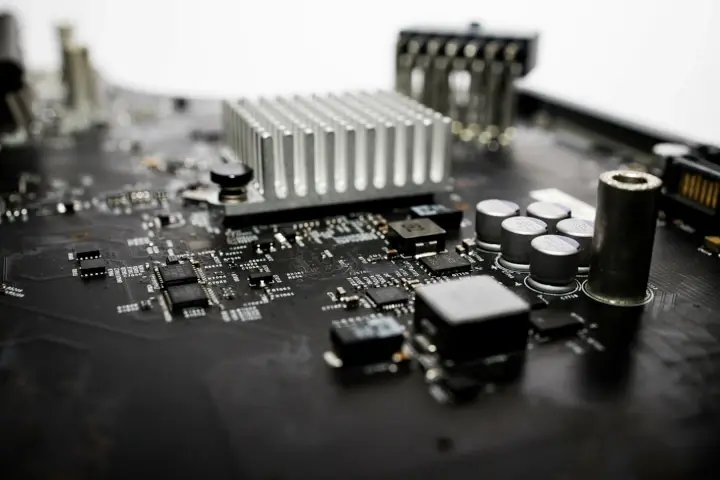
Loaded PCBAs, also known as assembled or populated PCBs, are printed circuit boards with all the required electronic components mounted onto them. Once these components are soldered, the PCB assembly becomes a functional unit within an electronic device, facilitating electrical connections and interactions between the components.
However, circuit board faults can affect the overall performance of the assembled PCB in various ways. To apply effective circuit board testing methods, it’s important to understand these faults. Here are three common categories:
- Component faults: Sometimes, electronic parts like resistors, capacitors, or integrated circuits don’t work as they should. These faults can come from low-quality materials, manufacturing mistakes, or damage during transportation or assembly.
- Manufacturing faults: During PCBA manufacturing, errors such as poor solder joints, misaligned components, incorrect placement, or insufficient solder paste application cause manufacturing faults.
- Performance faults: Sometimes, the PCBA does not perform as expected, even when everything else seems to be fine. Factors like a wrong circuit design, poor heat management, or electromagnetic interference can cause these faults.
With proper care, PCBA manufacturing involves few instances of faults. Nevertheless, advanced circuit board testing methods can pinpoint these anomalies when they occur.
Testing Circuit Boards Proactively Using Design for Testability (DFT)
As competition intensifies in the electronics industry, early fault identification is a linchpin for optimizing resource allocation, thereby maximizing return on investment. The ability to catch and rectify defects early can provide exponential savings in time, effort, and capital, offering businesses a strategic edge. One proactive approach to facilitate efficient testing of PCBAs is the concept of Design for Testability (DFT).
DFT involves a proactive and innovative design strategy, shaping electronic circuits and components with testing and troubleshooting in mind. This makes it easier to identify and correct potential issues during manufacturing. By incorporating DFT principles, engineers can improve the test coverage and streamline the testing process while enhancing overall product quality and time-to-market. Key elements of DFT include
- Test Point Accessibility: Ensuring that test points, or the specific locations on a PCBA where testing equipment connects, are easily accessible is crucial in DFT. Proper test point placement allows efficient testing with minimal interference from adjacent components. Maintain a separation between tall components and test points on the board in order to avoid interference.
- Testability Features: Incorporating testability features, such as built-in self-test (BIST) circuits, can help detect and diagnose faults more effectively. These features make testing a device’s functionality possible without the need for extensive external testing equipment. It is more common for critical systems that cannot fail to have BIST circuits.
- Design Simplicity: Simplifying the PCBA design by reducing the complexity of circuitry and components can make testing and troubleshooting more manageable. This can be achieved by using modular designs or minimizing the number of unique components.
- Design Hierarchies: Organizing a PCB design into functional blocks or modules can enhance testability. By dividing the PCB layout into smaller, independent sections, engineers can more easily identify and resolve the source of a fault. Additionally, if a company reuses functional blocks, it can design faster and experience fewer performance issues.
- Adequate Spacing and Component Layout: Maintaining proper spacing between components and optimizing their layout can minimize potential interference, making testing more effective. This also reduces the likelihood of faults caused by components being too close together or generating excess heat.
Now that we’ve explored the importance of identifying faults in loaded PCB assemblies and the value of incorporating Design for Testability principles, let’s examine the actual methods of testing circuit boards.
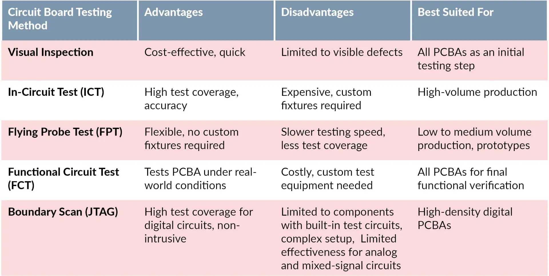
Common Circuit Board Testing Methods
Here is a summary table that briefly compares the advantages and disadvantages of each testing method, along with the situations they are best suited for. Keep in mind that a combination of these methods may be employed depending on your project’s specific requirements and constraints.
Visual Inspection
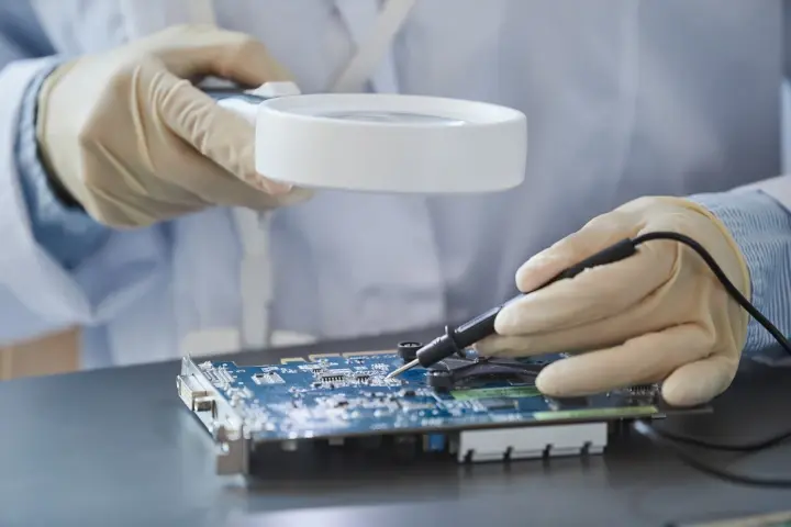
Visual inspection, as the name suggests, involves examining the PCBA for defects using the naked eye, magnification tools, or the increasingly popular automated optical inspection (AOI) systems. AOI systems employ sophisticated cameras and software algorithms to scan the PCBA and identify defects automatically.
Being the initial step in the testing process, Visual Inspection can promptly highlight a range of issues, including misaligned components, solder bridging, or missing/damaged parts. While this method offers quick results and is cost-effective, it does have its limitations. It may overlook faults that aren’t apparent to the naked eye, or those concealed beneath components.
In-Circuit Test (ICT)
The In-Circuit Test (ICT) method involves using a specialized testing device, known as a “bed of nails” fixture. This fixture establishes an electrical connection with designated test points on the PCBA.
ICT equipment gauges electrical properties like resistance, capacitance, and inductance to detect faults such as short circuits, open circuits, or incorrect component values. ICT provides impressive test coverage and accuracy, but it requires the development of a custom test fixture for each PCBA design, a process that can be time-consuming and expensive.
Flying Probe Test (FPT)
The Flying Probe Test (FPT) is a non-contact method that uses a set of movable probes to make electrical contact with test points on the PCBA.These probes traverse the board, systematically testing each point following a pre-defined sequence.
Like ICT, FPT measures electrical properties to detect faults. However, unlike ICT, FPT does not require a custom fixture, making it a more cost-effective and flexible option for low to medium-volume production or prototypes. A notable downside to FPT is that it is slower compared to ICT, and it may not provide the same degree of test coverage.
Checkpoint
Catching and rectifying defects early can save businesses time, effort, and capital, giving them a competitive advantage.

Functional Circuit Test (FCT)
Functional Circuit Test (FCT) evaluates the overall functionality of the assembled PCBA by applying power and input signals and measuring the output signals. In other words, FCT tests the board under conditions that simulate its actual operation in the end product. This method can identify performance faults and confirm that the PCBA operates as intended.
However, functional testing requires the development of custom test equipment and software, which can be costly and time-consuming. Additionally, it may not identify the specific location of a fault, making troubleshooting more challenging.
Boundary Scan (JTAG)
Boundary Scan, also recognized as the Joint Test Action Group (JTAG), is a testing technique that relies on embedded test circuits within the components themselves. These test circuits link up to form a “boundary scan chain,” enabling the tester to directly access and evaluate the functionality of components and interconnections.
JTAG is especially useful for testing boards with restricted physical access or a high density of components. This technique offers high test coverage and can identify faults that may elude other methods. However, it does require components with embedded boundary scan capabilities, and setting up a JTAG test can be a complex and time-consuming endeavor.
Selecting the Right PCB Testing Method
PCBA testing methods are crucial to making sure your electronic product works properly. For determining which testing method will work best for your order, your CM can assist you, but keep these factors in mind:
- Project Needs: Look at your project’s requirements, like testing accuracy, test coverage, and any special factors for your PCBA design. Think about the complexity of the circuit, the components you’re using, and how the PCBA will be used.
- Production Volume: How much you’re producing affects which testing method is best. For large production runs, In-Circuit Test (ICT) might be a better choice because it’s more accurate and covers more tests. But for smaller runs or prototypes, Flying Probe Test (FPT) gives you the flexibility you need without having to invest in custom equipment.
- Budget: Don’t forget about the cost of the testing method you pick. Some methods are more accurate and cover more tests, but they might need custom fixtures or equipment that can be expensive. Compare the costs of each testing method, including both upfront and long-term expenses, to find the best value.
- Test Accessibility: Take a look at the layout and design of your PCBA. Are there any limitations that could affect the testing method you choose? For example, Boundary Scan (JTAG) works great for high-density digital PCBAs with limited access, while other methods may work better for designs with easy access to test points.
- Turnaround Time: Think about how much time you have for your project. Some testing methods can take longer to set up and run. For example, ICT needs custom fixtures, which can take a while to create, while FPT is known for its quick setup time.
Achieving Cost-effective Test Coverage
Finding the right balance between test coverage and the cost is essential for circuit board testing. Generally, more thorough testing leads to better results. However, more comprehensive testing often comes with increased costs, such as custom fixtures, test equipment, or longer testing times.
To strike the right balance, consider the following:
- Prioritize crucial tests: Identify the most critical tests for your specific PCBA design and focus on achieving high test coverage for those areas.
- Combine testing methods: Utilize a mix of testing methods to maximize test coverage while minimizing costs. For example, you can combine a cost-effective method like Visual Inspection with a more comprehensive method like ICT or FPT.
- Assess cost-effectiveness: Regularly evaluate the cost-effectiveness of your chosen testing methods, taking into account factors like production volume, budget constraints, and project requirements.
The key to developing a high-quality, reliable electronic product is to carefully balance test coverage and cost. If you don’t test, you may incur long-term costs, including increased returns as a result of more board defects slipping through the cracks, increased RMAs, increased fault-forward costs, reduced first-pass yields, increased service costs, and a loss of quality reputation. When assessing testing costs, keep these factors in mind.
Conclusion
To ensure the quality, reliability, and performance of electronic products, it’s important to have effective circuit board testing methods. We’ve explored several such methods, including Visual Inspection, In-Circuit Test (ICT), Flying Probe Test (FPT), Functional Circuit Test (FCT), and Boundary Scan (JTAG).
However, it’s not enough to simply rely on these testing methods alone. By considering your testing requirements early on in the design process, you can effectively balance test coverage, cost, and project needs. By doing so, you can consistently produce high-quality electronic products that meet your customers’ expectations.
Related Topics
PCBA Design: Five Tips to Clean Up Your Layout
Before sending your final design files to the CM for PCB manufacturing, check out these useful tips and final steps.
The Case for PCBAs Made in America
Companies looking to increase the agility, productivity, and resilience of their electronics supply chains can do so with local and regional vendors.
Manufacturing PCBAs in Mexico: Do it with American-Based MacroFab
For companies with midsize to large production runs looking for nearshoring advantages, switching to Mexico is a smart move.
Explore MacroFab's Testing Services
A quality hardware tech product depends on testing & inspection. MacroFab helps you get it right.
About MacroFab
MacroFab offers comprehensive manufacturing solutions, from your smallest prototyping orders to your largest production needs. Our factory network locations are strategically located across North America, ensuring that we have the flexibility to provide capacity when and where you need it most.
Experience the future of EMS manufacturing with our state-of-the-art technology platform and cutting-edge digital supply chain solutions. At MacroFab, we ensure that your electronics are produced faster, more efficiently, and with fewer logistic problems than ever before.
Take advantage of AI-enabled sourcing opportunities and employ expert teams who are connected through a user-friendly technology platform. Discover how streamlined electronics manufacturing can benefit your business by contacting us today.