The following are what MacroFab currently offers for PCB options through the online interface. See this knowledge base article for how to customize your PCB options.
PCB Specifications
These are what MacroFab currently offers for PCB options though the online interface. See this knowledge base article for how to customize your PCB options.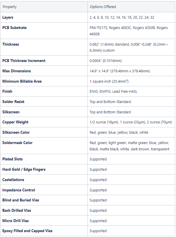
Silkscreen line width = 5mil
Design Rules for PCBs
MacroFab has 4 different sets of Design Rule Checks (DRC) for PCBs. Standard, Extended Manufacturing, Extended Drill, and Extended Manufacturing and Drill. Most PCBs fall under our Standard DRC.
DRC for 1oz (35μm) copper PCBs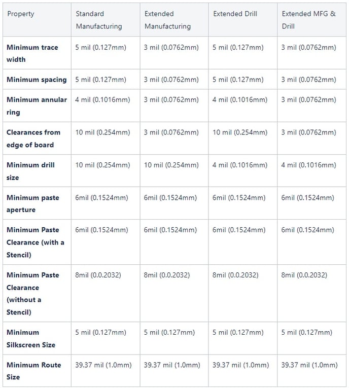
DRC for 2oz (70μm) copper PCBs
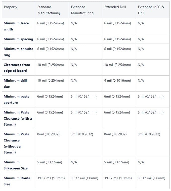
For PCBs with 2oz (35μm) copper the minimal trace width, spacing, and annular ring need to be larger to account for the thicker plating of copper. Because of this, 2oz Copper disables the extended manufacturing option.
Board Edge Routing
Our PCB Board Edge (Routing) Tolerance is ± 6mil (0.15mm).
Finished Drill Sizing
The MacroFab platform interprets drill hits as the finished size. This is the final diameter after plating and the surface finish applied. No plating tolerance is required in specifying drill sizes.
Drill Ratios and Laser Vias
The drill aspect ratio is the relationship between the depth of the drill hit and the width. For example, if the drill hit goes all the way through a 62 mil (1.6mm) thick PCB (standard PCB thickness) and the drill hit is 4 mil (0.1016mm) in diameter the ratio would be 62 ÷ 4 = 15.5.
| Drill Option | Max Drill Ratio |
|---|---|
| Standard Drills | 10 |
| Extended Drills | 16 |
Standard mechanical drills are used all the way down to 4 mil (0.1016mm) diameter vias. Laser drilling techniques are used for blind and buried vias.
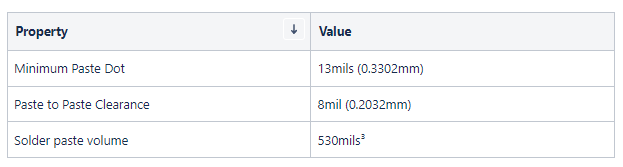
Paste Layer Specifications
Paste layers for PCB designs should be 1:1 ratio with the copper lands.
MacroFab utilizes a solder paste Jet Printer to help cut down the costs for our customers whenever we can. However, the minimum dot size it can print is 13mils. Due to this limitation a stencil may be required if the solder paste volume and/or paste dimensions are under these limits.
Jet Printer Specifications
Paste layer specifications that are below these limits will require the use of a solder paste stencil.
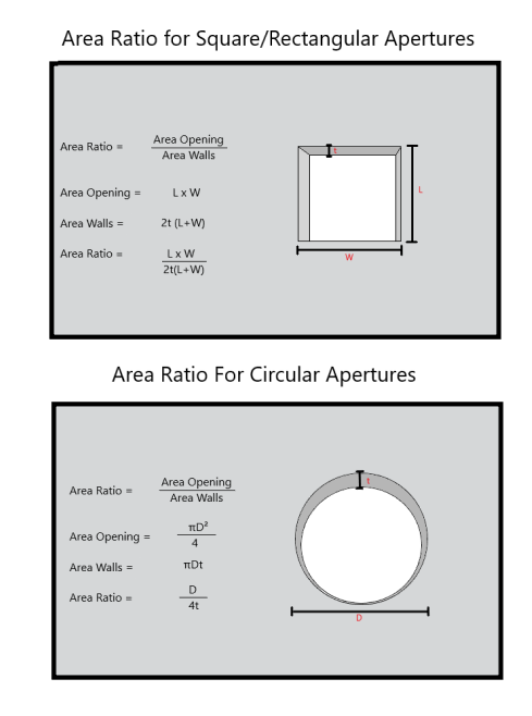
Stencil apertures and Advanced Nano coating
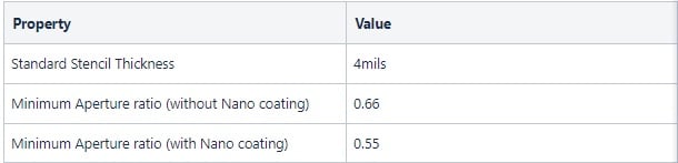
Some design apertures are too small for the solder paste to properly be deposited with a stencil. We identify this using area ratios. If the Area ratio is less than 0.66, we will require the use of Advanced Nano coating to ensure the solder paste deposits on the PCB lands and does not adhere to the sidewalls. The use of Advanced Nano can allow us to print apertures with a area ratio as low as 0.55. If you have an aperture with an area ratio less than 0.55, we can revise the aperture design or stencil thickness to meet our requirements.
What is Advanced Nano coating?
Advanced Nano is a highly unique and patented coating that is applied to the bottom side of the stencil and inside the apertures, the squeegee side remains uncoated. This advanced coating provides the stencil with anti-adhesion properties. Advanced Nano stencil utilizes a specialized 1-2 um hardened nano coating. This permanent hydrophobic coating repels solder flux allowing increased transfer of paste. Advanced Nano Stencils improve solder paste deposits which results in consistent paste transfer volumes and minimizes bridges which leads to higher process stability with lower failure rates.
PCB Layer Stack Ups
MacroFab has a standard set of PCB layer stack ups and supports custom stackups and PCB substrate materials for PCB Assemblies. For more information on PCB layer stack ups check out the knowledge base article PCB Layer Stack Ups and this blog about PCB Thickness.
PCB and Material Datasheets
Below you can find the datasheets for the materials that are used to create your PCB.
PCB Manufacturing Standards
FR4 datasheet
R-500 GHB Soldermask Datasheet
Assembly Capabilities
MacroFab's assembly capabilities can be found in this knowledge base article.
Additional Questions?
Our support and engineering staff is here to help! If you have any questions about your PCB design and what set of DRC to use, contact our support team! Does your PCB assembly need different specifications, material, or stack up other then what we offer? Contact our sales team today.