Creating PCB Assemblies from your KiCad PCB Project
If you use the EDA Tool KiCad to design your PCB Assemblies, the best way to build a new project is to upload the following files:
- pcbname.kicad_pcb
- The MacroFab Platform will extract the Gerber files (PCB design), placement of components, component footprints/values, and Part Numbers for components from this file.
- Bill of Materials from a .XLSX spreadsheet (optional)
- Instead of, or in addition to, the pcbname.sch file from your project, you can upload a Bill of Materials as a spreadsheet.
- pcbname.sch (optional - only supported for KiCad v5 and older)
- The MacroFab Platform will extract Part Numbers for components from this file if they are present. Note MacroFab does not support the kicad_sch format as all of the manufacturing data needed is also stored in kicad_pcb for KiCad v6 and newer.
Once you have created this manufacturing package you will be able to easily upload your PCB Assembly to the MacroFab platform.
NOTE: For versions v6 and later, MacroFab does not support the .kicad_sch or .sch format. The manufacturing data is stored in the kicad_pcb file on v6 and later and the schematic files are no longer needed for design import.
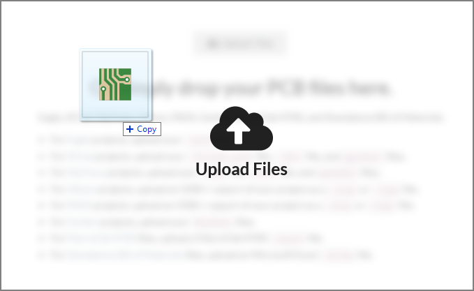
In the Design tab, simply drag-and-drop your KiCad manufacturing package into the file upload target. Alternatively, you can click the Upload Files button on the right side of the screen. More information about uploading files to the platform can be found on the knowledge base article Creating a PCB and Uploading Design Files.
Recording Manufacturer's Part Numbers in Your Design
With KiCad, you can either maintain your part numbers in a separate excel file, or you can record the manufacturer's part number directly in your design. By recording the part number directly in your design, MacroFab can extract this information when you upload your .sch file. Maintaining the part numbers in your design minimizes the number of documents you have to manage.
To record the manufacturer's part number in your design and have the MacroFab platform automatically extract it from your .sch file, you'll need to add a custom field to the part in the schema editor. To do so, open eeschema, find the component you want to record the part number for and edit the Symbol Properties. You'll want to add a new property for the part number and, optionally, whether or not to populate it.
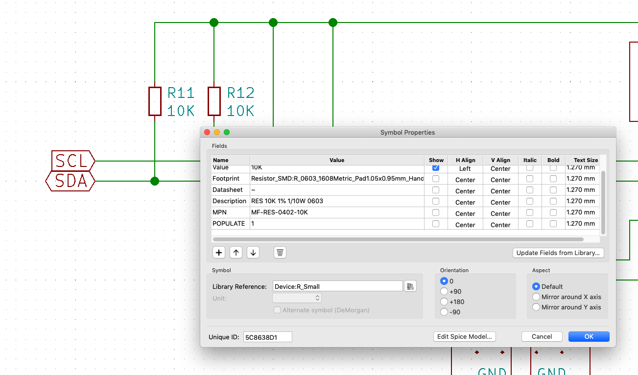
To set the part number, add a property named 'mpn' or 'part number' and set the value to be the part number you wish to use. The following properties are automatically parsed by the MacroFab platform:
- mpn
- The value will be parsed as the selected part number
- part number
- The value will be parsed as the selected part number
- populate
- If the value is 1, the part will be populated; 0 means do not populate
- dnp
- Opposite of populate -- 1 means do not populate, 0 means populate
The default for all parts is to populate them.
Note: all property names are case-insensitive.
Manually Generating Required Manufacturing Data
If you'd rather generate drills, gerbers, and bill of materials manually, that is possible. KiCad does not allow you to use a configuration file for generating manufacturing data, so we will walk you through the process below.
The .Kicad_PCB File
For our process to know where your components on your PCB Assembly are placed and the size of the components, we require the .kicad_pcb file from your PCB project. When the .kicad_pcb file is uploaded to the MacroFab platform the placement locations, values, and footprints of all components will automatically be extracted.
PCB Layer Gerber File Generation
Gerber files have to be generated manually from KiCad. Open up the plot menu by clicking on File then Plot. Make sure the following layers are selected: F.Cu, B.Cu, F.Paste, B.Paste, F.SilkS, B.SilkS, F.Mask, B.Mask, Edge.Cuts. If you have internal layers (In1.Cu, In2.Cu, ect..) make sure these are selected as well. PCB layers can be renamed in KiCad so if they are renamed you will have to take care in selecting the correct layers.
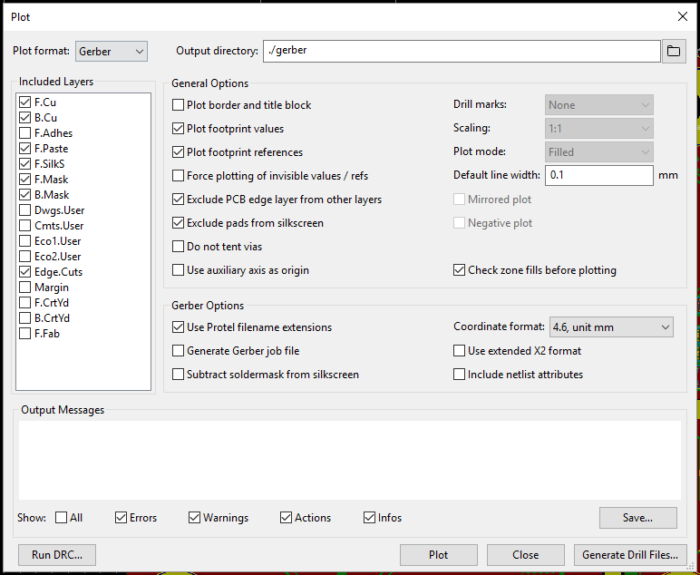
Before generating gerbers it is generally a good idea to run KiCad's Design Rule Check. See the section below on how to run DRC.
Click the Plot button at the bottom of the window and KiCAD will generate the Gerber files. Next, the drill file needs to be created. Open the Drill Files Generation window by clicking the Generate Drill File at the bottom of the Plot window.
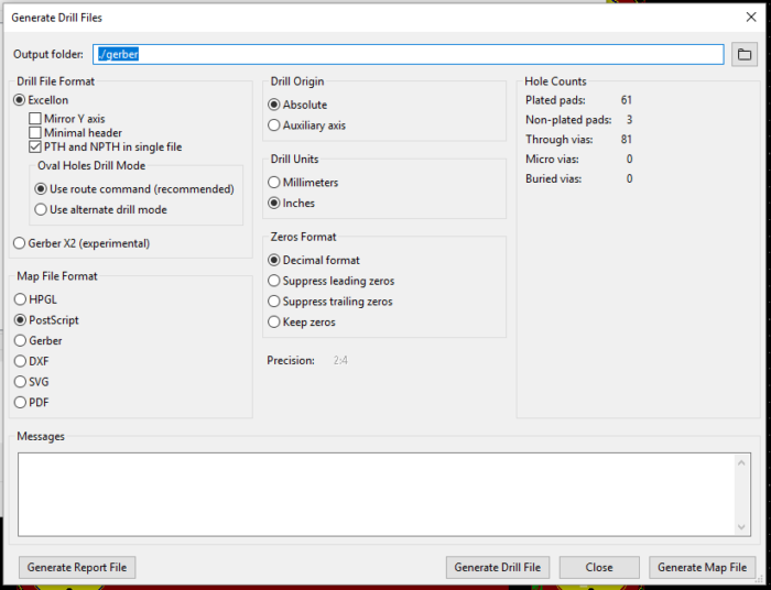
Make sure the options are the same as shown above, then click Drill File which will generate the Excellon Drill file required.
Gerber File Extension Names
Double-check the extension names that KiCad generated for the gerber files. They should match the file extensions listed in the Required Design Files article. If the gerber file extensions do not match what the platform expects, the gerbers will not be processed automatically and you will need to organize the layers in the platform using the Design Viewer.
Bill of Materials Generation
For the Bill of Materials Auto Fill to work on the MacroFab Platform, Manufacture Part Numbers (MPNs) must be supplied for the components. You can either upload the .sch file from your KiCad project, or use a separate spreadsheet. The spreadsheet only needs to contain designators and the corresponding MPN. For more information on making an XLSX formated spreadsheet and uploading it see the knowledge base article, Importing a Bill of Materials Spreadsheet.
Design Rule Check (DRC)
To setup the design rules in KiCad open Pcbnew and click the File menu at the top. Select Board Setup... from the drop menu. The Board Setup window will appear and there is a section for Design Rules. You will be able to input the DRC settings for MacroFab here.
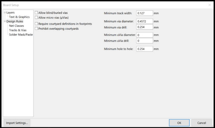
Minimum via diameter is the minimum drill diameter plus two times the minimal annular ring. EX: 10mil + 2*(4 mil ) = 18mil or 0.4572 mm
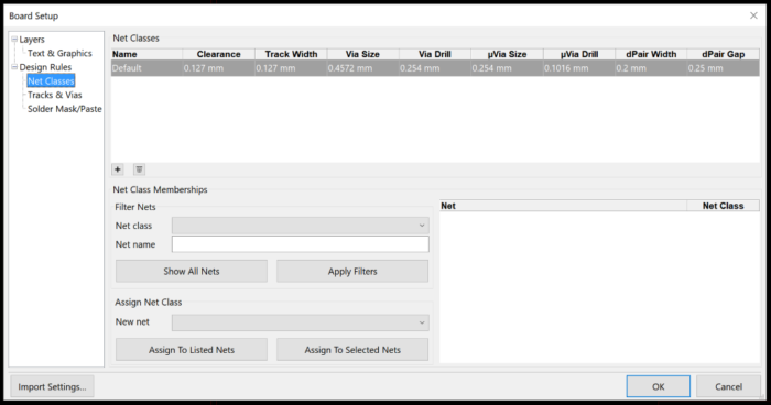
You will also need to edit the Default Net List rules with the DRC Settings.
Please note! Our most up-to-date DRC settings can be found on the PCB Specifications and DRC page.
Cut Outs, Routs, and Slots
The MacroFab Platform currently only works with internal cut outs, routs, and slots that are defined as gerber features. To make this work in KiCad, cut outs, routs, and slots will need to be defined on the Edge.Cuts layer. This causes the cut outs, routs, and slots to be combined with the border layer gerber file. The MacroFab platform currently does not support drill slots. For more information about cut outs, slots, routes, and board outlines check out this engineering article.
Additional KiCad Questions?
If you have any other questions about creating a PCB Assembly with a KiCad PCB Project please contact our support team.